
Specifications
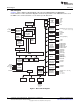


Standard Initialization Sequence for Hercules Microcontrollers
www.ti.com
2.8 Run Self-Test on the eFuse Controller SECDED Logic
Electrically programmable fuses (eFuses) are used to configure the part after de-assertion of power-on
reset (nPORRST). The eFuse values are read and loaded into internal registers as part of the power-on-
reset sequence. This is called the eFuse autoload. The eFuse values are protected with single-bit error-
correction, double-bit error-detection (SECDED) codes. These fuses are programmed during the initial
factory test of the device. The eFuse controller is designed so that the state of the eFuses cannot be
changed once the device is packaged.
For safety critical systems, it is important for the application to check the status of the eFuse controller
after a device reset. For more details on eFuse controller errors and the application sequence to check for
these errors, see the eFuse Controller chapter of the device-specific technical reference manual.
2.9 Release Reset and Clocks to Peripherals
The peripherals are kept under reset, and need to be explicitly brought out of reset by the application. This
can be done by setting the peripheral enable (PENA) bit of the Clock Control Register (CLKCNTL).
The clocks to the peripheral modules are also disabled upon any system reset and need to be explicitly
enabled by the application. This can be done by setting the bits corresponding to the peripheral select
quadrant occupied by the peripheral module in the Peripheral Central Resource (PCR) Control Registers
for clearing the power down states of peripheral modules (Peripheral Power-Down Clear Register [0:3]
(PSPWRDWNCLRx)). For information on the peripheral select quadrants for each peripheral, see the
device-specific data sheet.
2.10 Configure Flash Access
The Flash memory on the TMS570LS043x, TMS570LS033x, and RM42L432 series of microcontrollers is
a non-volatile electrically erasable and programmable memory.
The TMS570LS043x, TMS570LS033x, and RM42L432 series of microcontrollers contain a digital module
that manages all accesses to the Flash memory. A Flash access can be completed without any wait states
required for bus master clock speeds up to 45 MHz. If the bus clock is faster than 45 MHz, then any Flash
access requires the appropriate number of wait states depending on the bus clock speed. The
TMS570LS043x, TMS570LS033x, and RM42L432 series of microcontrollers support clock speeds up to
80 MHz for the TMS570LSxx3x devices and up to 100MHz for the RM42L432 device. For the actual
maximum allowed speed and the number of corresponding address and data wait states, see the device-
specific data sheet.
Suppose that the application requires a CPU clock speed of 80 MHz. This requires 1 data wait state and
no address wait states for any access to the Flash memory. These wait states need to be configured in
the Flash module registers.
The Flash module also features a pipelined mode of operation. When this mode is enabled, the module
reads 128 bits from the Flash memory and holds them in buffers that the CPU can read from without any
wait state. The CPU can read 32 or 64 bits of instructions or data from the pipeline buffers.
The Flash Read Control Register (FRDCNTL) inside the Flash module controls the wait states and the
pipeline mode.
The TMS570LS043x, TMS570LS033x, and RM42L432 series of MCUs also have a separate Flash bank
(bank number 7) that is dedicated for data storage. This bank has a different architecture that is intended
specifically to be used to emulate an EEPROM with software. Accesses to this Flash bank is configured
via a separate EEPROM Emulation Configuration Register (EEPROM_CONFIG) in the Flash module. A
write operation to the EEPROM_CONFIG register must first be enabled by configuring the Flash State
Machine Write Enable Control Register (FSM_WR_ENA).
Once the access to the FSM control registers is enabled, the read access to the Flash bank 7 can be
configured to accommodate the bank number 7 specific wait states for the selected device operating
frequencies. Reference the device specific datasheet for the appropriate number of wait states needed for
bank 7 accesses.
8
Initialization of the TMS570LS043x, TMS570LS033x and RM42L432 SPNA163–September 2012
Hercules ARM Cortex-R4 Microcontrollers
Submit Documentation Feedback
Copyright © 2012, Texas Instruments Incorporated