
Specifications


www.ti.com
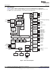
Standard Initialization Sequence for Hercules Microcontrollers
Table 1. Clock Sources on Hercules Microcontrollers (continued)
Clock
Source
Number Clock Source Name Description
No clock signal is connected to source 2. This clock source must not be enabled or
2 Not implemented
chosen for any clock domain.
External clock input. This clock source must only be enabled if there is an actual
3 EXTCLKIN external clock source connected to the identified device terminal for EXTCLKIN. For
more information, see the device-specific data sheet.
This is the low-frequency output of the internal reference oscillator. The LF LPO is
4 LF LPO
typically an 80 KHz signal, and is generally used for low-power mode use cases.
This is the high-frequency output of the internal reference oscillator. The HF LPO is
5 HF LPO typically a 10 MHz signal, and is used as a reference clock for monitoring the main
oscillator.
No clock signal is connected to source 6. This clock source must not be enabled or
6 Not Implemented
chosen for any clock domain.
No clock signal is connected to source 7. This clock source must not be enabled or
7 Not Implemented
chosen for any clock domain.
2.7.2 Control Registers for Enabling and Disabling Clock Sources
There are five available clock sources on the TMS570LS043x, TMS570LS033x, and RM42L432 series of
microcontrollers:
• Clock sources 0, 4 and 5 are enabled, while clock sources 1 and 3 are disabled upon any system
reset.
• Clock sources 2, 6, and 7 are not implemented and must not be enabled in the application.
• Each bit of the system module Clock Source Disable Register (CSDIS) controls the clock source of the
same number: bit 0 controls clock source 0, bit 1 controls clock source 1, and so on.
• There are also dedicated Clock Source Disable Set (CSDISSET) and Clock Source Disable Clear
(CSDISCLR) registers to allow the application to avoid using read-modify-write operations.
• Setting any bit commands, the corresponding clock source to be disabled.
– The clock source can only be disabled once there is no clock domain or secondary clock source
(FMPLL) using the clock source to be disabled.
2.7.3 Example Clock Source Configuration
systemREG1->CSDISCLR = 0x00000000U
| 0x00000001U // Enable clock source 0
| 0x00000002U // Enable clock source 1
| 0x00000010U // Enable clock source 4
| 0x00000020U; // Enable clock source 5
The above configuration enables clock sources 0, 1, 4, and 5.
Of the clock sources that are enabled, numbers 0, 4 and 5 are enabled by default and will have become
valid by the time the processor is released from reset upon a power-up. These are the main oscillator and
the two outputs from the internal reference oscillator.
Clock source 1 is the PLL output. The FMPLL has a defined start-up time, and its output is not available
for use until this time. The application must wait for the valid status flag for this clock source to be set
before using the FMPLL output for any clock domain. The example initialization sequence makes use of
this FMPLL lock time to perform all initialization actions that don't have to be done at the maximum
operating frequency chosen for the application.
7
SPNA163–September 2012 Initialization of the TMS570LS043x, TMS570LS033x and RM42L432
Hercules ARM Cortex-R4 Microcontrollers
Submit Documentation Feedback
Copyright © 2012, Texas Instruments Incorporated