
Specifications


/NR
/1 to /64
OSCIN
PLL
INTCLK
/OD
/1 to /8
VCOCLK
/R
/1 to /32
post_ODCLK
/NF
/1 to /256
PLLCLK
f
PLLCLK
= (f
OSCIN
/ NR) * NF / (OD * R)
Standard Initialization Sequence for Hercules Microcontrollers
www.ti.com
2.6 Configure PLLs
The TMS570LS043x, TMS570LS033x, and RM42L432 series of microcontrollers contain a frequency-
modulated phase-locked loop (FMPLL) macro that allows the input oscillator frequency to be multiplied to
a higher frequency than can be conveniently achieved with an external resonator or crystal. Additionally,
the FMPLL allows the flexibility to generate many different frequency options from a fixed crystal or
resonator.
The FMPLL allows the application to superimpose a “modulation frequency” signal on the selected base
frequency signal output from the FMPLL. This reduces the electromagnetic energy of the output signal by
spreading it across a controlled frequency range around the base frequency. This mode is disabled by
default, and the application can enable it in applications sensitive to noise emissions.
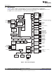
2.6.1 FMPLL Block Diagram
Figure 2 shows a high-level block diagram of the FMPLL macro.
Figure 2. FMPLL Block Diagram
The parameters f
OSCIN
, f
post_ODCLK
and f
HCLK
are data sheet specifications. To identify the minimum or
maximum limits on these frequencies, see the device-specific data sheet.
NOTE: The FMPLL takes (127 + 1024*NR) oscillator cycles to acquire lock to the target frequency,
hence it is recommended to configure the FMPLL(s) and enable them as soon as possible in
the device initialization.
2.6.2 FMPLL Configuration
PLL1 is configured using two control registers, PLL Control 1 Register (PLLCTL1) and PLL Control 2
Register (PLLCTL2), located within the System module on the Hercules microcontrollers.
2.7 Enable Clock Sources
2.7.1 Available Clock Sources on Hercules Microcontrollers
The TMS570LS043x, TMS570LS033x, and RM42L432 series of microcontrollers support five different
clock sources, as listed in Table 1.
Table 1. Clock Sources on Hercules Microcontrollers
Clock
Source
Number Clock Source Name Description
This is the primary oscillator, typically driven by an external resonator or crystal. This
0 OSCIN is the only available input to the FMPLL and the FMPLL2 macros. The OSCIN
frequency must be between 5 MHz and 20 MHz.
This is the output of the FMPLL, which is generated using the OSCIN as the input
clock. The FMPLL output clock frequency must not exceed the maximum device
1 FMPLL#1 output frequency specified in the device-specific data sheet. The FMPLL features a
modulation mode where a modulation frequency is superimposed on the FMPLL
output signal.
6
Initialization of the TMS570LS043x, TMS570LS033x and RM42L432 Hercules SPNA163–September 2012
ARM Cortex-R4 Microcontrollers
Submit Documentation Feedback
Copyright © 2012, Texas Instruments Incorporated