
Specifications


www.ti.com
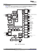
Standard Initialization Sequence for Hercules Microcontrollers
The CPU’s call-return stack consists of a 4-entry circular buffer. When the CPU pre-fetch unit (PFU)
detects a taken procedure call instruction, the PFU pushes the return address onto the call-return stack.
The instructions that the PFU recognizes as procedure calls are, in both the ARM
®
and Thumb instruction
sets:
→ BL immediate
→ BLX immediate
→ BLX Rm
When the return stack detects a taken return instruction, the PFU issues an instruction fetch from the
location at the top of the return stack, and pops the return stack. The instructions that the PFU recognizes
as procedure returns are, in both the ARM and Thumb instruction sets:
→ LDMIA Rn{!}, {..,pc}
→ POP {..,pc}
→ LDMIB Rn{!}, {..,pc}
→ LDMDA Rn{!}, {..,pc}
→ LDMDB Rn{!}, {..,pc}
→ LDR pc, [sp], #4
→ BX Rm
2.2 Enable Response to ECC Errors in Flash Interface Module
The Flash module has a Flash Error Detection and Correction Control Register 1 (FEDACCTRL1) at
address 0xFFF87008. This register controls the ECC functionality implemented inside the Flash module,
including support for the SECDED logic inside the Cortex-R4 CPU. The bits 3–0 of this register make up
the EDACEN field. EDACEN is configured to 0x5 by default. The application must configure EDACEN to
0xA in order to enable the Flash module's support for the CPU's SECDED logic.
2.3 Enable the Cortex-R4 CPU’s Event Signaling Mechanism
The Cortex-R4 CPU has a dedicated event bus that is used to indicate that an event has occurred. This
event signaling is disabled upon reset and must be enabled. The Flash module and the RAM module
interfaces capture the ECC error events signaled by the CPU. This allows the application to further debug
the exact address, which caused the ECC error.
The CPU event signaling can be enabled by clearing the “X” bit of the performance monitoring unit’s
“Performance monitor control register, c9”.
2.4 Enable the Cortex-R4 CPU’s ECC Checking for ATCM Interface
The CPU has internal ECC logic that protects all CPU accesses to the ATCM (Flash) interface. This logic
is not used by default and must be enabled by setting the ATCMPCEN bit of the System control
coprocessor’s Auxiliary control register, c1.
2.5 Handle the Cause of Reset
Each application has different levels of tolerance for different reset conditions. A typical reset handler is
presented in the accompanying example code project, which identifies all the causes of a reset condition
on the Hercules MCUs.
5
SPNA163–September 2012 Initialization of the TMS570LS043x, TMS570LS033x and RM42L432
Hercules ARM Cortex-R4 Microcontrollers
Submit Documentation Feedback
Copyright © 2012, Texas Instruments Incorporated