
User guide


Programmers Model
ARM DDI 0337I Copyright © 2005-2008, 2010 ARM Limited. All rights reserved. 3-11
ID072410 Non-Confidential
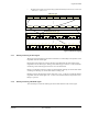
3.4 System address map
The processor contains a bus matrix that arbitrates the processor core and optional Debug
Access Port (DAP) memory accesses to both the external memory system and to the internal
System Control Space (SCS) and debug components.
Priority is always given to the processor to ensure that any debug accesses are as non-intrusive
as possible. For a zero wait state system, all debug accesses to system memory, SCS, and debug
resources are completely non-intrusive.
Figure 3-1 shows the system address map.
Figure 3-1 System address map
Table 3-2 shows the processor interfaces that are addressed by the different memory map
regions.
System
External device
External RAM
Peripheral
SRAM
Code
0xFFFFFFFF
Private peripheral bus - External
0xE0100000
0xE0040000
0xA0000000
0x60000000
0x40000000
0x20000000
0x00000000
ROM Table
ETM
TPIU
Reserved
SCS
Reserved
FPB
DWT
ITM
External PPB
0xE0042000
0xE0041000
0xE0040000
0xE000F000
0xE000E000
0xE0003000
0xE0002000
0xE00FF000
0x40000000
Bit band region
Bit band alias
32MB
1MB
31MB
0x40100000
0x42000000
0x44000000
0xE0001000
0xE0000000
Private peripheral bus - Internal
Bit band region
Bit band alias
32MB
1MB
31MB
0x20000000
0x20100000
0x22000000
1.0GB
1.0GB
0.5GB
0.5GB
0.5GB
0xE0000000
0xE0100000
0xE0040000
0x24000000
Table 3-2 Memory regions
Memory Map Region
Code Instruction fetches are performed over the ICode bus. Data accesses are performed over the DCode bus.
SRAM Instruction fetches and data accesses are performed over the system bus.
SRAM bit-band Alias region. Data accesses are aliases. Instruction accesses are not aliases.
Peripheral Instruction fetches and data accesses are performed over the system bus.