
User guide


Programmers Model
ARM DDI 0337I Copyright © 2005-2008, 2010 ARM Limited. All rights reserved. 3-4
ID072410 Non-Confidential
3.3 Instruction set summary
This section provides information on:
• Cortex-M3 instructions
• Load/store timings on page 3-8
• Binary compatibility with other Cortex processors on page 3-9.
3.3.1 Cortex-M3 instructions
The processor implements the ARMv7-M Thumb instruction set. Table 3-1 shows the
Cortex-M3 instructions and their cycle counts. The cycle counts are based on a system with zero
wait states.
Within the assembler syntax, depending on the operation, the
<op2>
field can be replaced with
one of the following options:
• a simple register specifier, for example
Rm
• an immediate shifted register, for example
Rm, LSL #4
• a register shifted register, for example
Rm, LSL Rs
• an immediate value, for example
#0xE000E000
.
For brevity, not all load and store addressing modes are shown. See the ARMv7-M Architecture
Reference Manual for more information.
Table 3-1 uses the following abbreviations in the Cycles column:
P The number of cycles required for a pipeline refill. This ranges from 1 to 3
depending on the alignment and width of the target instruction, and whether the
processor manages to speculate the address early.
B The number of cycles required to perform the barrier operation. For
DSB
and
DMB
,
the minimum number of cycles is zero. For
ISB
, the minimum number of cycles
is equivalent to the number required for a pipeline refill.
N The number of registers in the register list to be loaded or stored, including PC or
LR.
W The number of cycles spent waiting for an appropriate event.
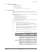
Table 3-1 Cortex-M3 instruction set summary
Operation Description Assembler Cycles
Move Register
MOV Rd, <op2>
1
16-bit immediate
MOVW Rd, #<imm>
1
Immediate into top
MOVT Rd, #<imm>
1
To PC
MOV PC, Rm
1 + P
Add Add
ADD Rd, Rn, <op2>
1
Add to PC
ADD PC, PC, Rm
1 + P
Add with carry
ADC Rd, Rn, <op2>
1
Form address
ADR Rd, <label>
1