GP4020 GPS Baseband Processor Design Manual Publication Number: DM5280 Issue: 3 Revision: 002 Issued: January 2002 Zarlink Semiconductor, Cheney Manor Swindon, Wiltshire, United Kingdom, SN2 2QW
Manual Revision History Version Revision Date Update Summary 1 001 February 2000 First Version 2 001 August 2000 GND and VDD pins marked as type “PWR” in tables 2.2 and 20.1. Modified TESTMODE (pin 74) definition. TM ® Removal of extra " " and " " trade-markings throughout. New BSIO Introduction (Secs 6.1, 6.2) Extensive DMAC usage procedures added (Sec 8) and section 17.4 deleted. Updated MPC Configuration for Memory Area 3 (Sec 11) New Note 1 added in Section 14.6.
Contents Page Contents .........................................................................................................................................iii Related Products and Documents.................................................................................................... v Trademarks .................................................................................................................................... v Document References..................................................
8.3 8.4 9 DMAC Triggering................................................................................................................ 99 Cautionary Notes .............................................................................................................. 101 GENERAL PURPOSE INPUT OUTPUT (GPIO) INTERFACE ....................................... 103 9.1 9.2 9.3 Introduction ......................................................................................................................
19.2 GP4020 Firefly MF1 Address Map..................................................................................... 183 20 INPUT / OUTPUT PIN CHARACTERISTICS ................................................................. 185 20.1 20.2 20.3 20.4 Pin Types ......................................................................................................................... 185 Input Delays ...........................................................................................................
Document References References to the following documents are made within the GP4020 GPS Baseband Processor Design Manual: 1) "ARM7TDMI Technical Reference Manual" ARM DDI 0029F, Rev 4 Copyright ARM Limited 2001. Arm Ltd. Documentation website (http://www.arm.
1: Introduction 1 INTRODUCTION 1.1 GP4020 GPS Baseband Processor Overview This design manual describes the GP4020 GPS Baseband Processor, which is based on the Zarlink Semiconductor Firefly MF1 Microcontroller Core (ref. Firefly MF1 Core Design Manual (DM5003)), and a custom Navstar GPS C/A code 12-channel spread-spectrum correlator. The GP4020 is a complete digital baseband processor for a Global Positioning System (GPS) receiver.
1: Introduction GP4020 BuILD BUS GPIO WATCH_EN WATCH_INT WATCH_TM NRESET WDOG UART_CLK TEST TESTMODE MULTI_FNIO GPIO[7:0] GPIO[7:0] DISCIO NSRESET Functional Description POWER_GOOD RTC_CLK REAL TIME CLOCK RTC_CMP_INT RTC_XIN RTC_XOUT GPIO[7:0] NRESET PLL PLLDT1 PLLAT1 UART_CLK BSIO PERIPHERAL CONTROL LOGIC BSIO PR_XIN NPOR_RESET TEST POWER CONTROL LINES DISCOP NRESET SYSTEM CLOCK GENERATOR UART_INT CLK_T UIM BUS DISCIO / DISCIP1 UART_CLK BuILD_CLK PR_XOUT CLK_I CK100K
1: Introduction 1.3.1 ARM Processor (ARM7TDMI) The ARM7TDMI is a 32-bit RISC microprocessor core designed by Advanced RISC Machines (ARM). It uses a series 7 microprocessor Core, with the following functional extensions: • Thumb (16-bit) instruction set • Debug interface-using J-TAG. • Fast Multiplier • Embedded In-Circuit-Emulation capability The ARM7TDMI is object-code compatible with all earlier ARM6 and ARM7 based products.
1: Introduction Details can be found in section 6 "BµILD SERIAL INPUT OUTPUT (BSIO) INTERFACE" on page 33. 1.3.5 12 Channel Correlator (CORR) This module contains 12 channels of PRN code correlators for spread-spectrum correlation of 12 simultaneous signals. Each channel contains an independent carrier DCO to allow independent mix down of a satellite signal to base-band before code correlation occurs. The correlator is designed to extract data modulated at a nominal chipping-rate of 1.
1: Introduction 1.3.9 General Purpose Input Output (GPIO) This module provides eight I/O pins, which may be bit or byte addressed and configured in a latched or transparent mode. When in byte mode, buffer full/empty flags are available which can be used to generate an interrupt to the ARM7TDMI processor. Details can be found in section 9 "GENERAL PURPOSE INPUT OUTPUT (GPIO) INTERFACE" on page 103. 1.3.
1: Introduction Since the internal SRAM is high-speed, it can be accessed with Zero wait-states through the Memory Peripheral Controller. Refer to section 11 "MEMORY PERIPHERAL CONTROLLER (MPC)" on page 109, for more information. 1.3.14 Real Time Clock (RTC) The GP4020 Real Time Clock uses an external 32kHz crystal to give an indication of time to the GP4020 chip, when the device is in Reset / Power Down.
1: Introduction Further details of the function and programming System Services Module can be found in Sections 2 and 8 of the "Firefly MF1 Core Design Manual" DM5003, available from Zarlink Semiconductor. 1.3.17 System Timer/Counters (SYSTIC) Two dual independent 32-bit timer/counters, with an 8-bit pre-scaler capability for each counter, are provided (Timers 1A, 1B, 2A and 2B). These are synchronous to the system clock and may be polled, or set-up to generate interrupts on over-run, with auto-reload.
8 TCXO 10MHz 35MHz SAW FILTER 175MHz LC FILTER (8) PREF CLK MAG SIGN LD OPCLK- OPCLK+ GP2015 1575MHz RF FILTER 1k 470 470 10nF 100k 100k 10k (70) (67) (63) (62) (61) (64) (56) (75) 100k (59) (58) 100k RTC_ XOUT (73) SAMPCLK IDDQTEST TEST RESET LOGIC BuILD _CLK BOOT ROM RAW TIMEMARK 12 CHANNEL CORRELATOR SAMPCLK MAG0 MAG0 SIGN0 SIGN0 POWER_GOOD RF_PLL_LOCK NSRESET SYSTEM CLOCK GENERATOR CLK_I WITH PLL CLK_T REAL TIME CLOCK RTC_ XIN (72) 10M 10pF M_CL
1: Introduction Figure 1.2 above shows a typical GPS receiver employing a GP2015 RF front–end, and a GP4020 correlator. The RF section, GP2015, performs down conversion of the L1 (1575.42MHz) signal for digital baseband processing. The resultant signal is then correlated in the GPS correlator within the GP4020 with an internally generated replica of the satellite PRN code to be received.
1: Introduction This page intentionally left blank.
2: GP4020 Package and Electrical Connections 2 GP4020 PACKAGE AND ELECTRICAL CONNECTIONS 2.1 GP4020 100-pin Package Dimensions The GP4020 GPS Baseband Processor is available from Zarlink Semiconductor in a 100-pin gull-wing Thin Quad Flat Package (TQFP). Ordering information for the GP4020 are shown in the “GP4020 GPS Baseband Processor Datasheet” DS5134, available from Zarlink Semiconductor. Figure 2.1 below shows the pin distribution around the package. Figure 2.
2: GP4020 Package and Electrical Connections Figure 2.
2: GP4020 Package and Electrical Connections Symbol Dimensions in millimetres MIN Nominal MAX A 1.40 1.60 A1 0.05 0.15 A2 1.35 1.45 D 15.80 16.20 D1 13.80 D3 14.20 12.00 E 15.80 16.20 E1 13.80 14.20 E3 12.00 L 0.45 e 0.75 0.50 b 0.17 0.27 c 0.09 0.20 Table 2.1 GP4020 100-pin package dimensions 2.2 GP4020 100-pin Package Electrical Connection Details All Vdd and GND pins must be connected to ensure reliable operation.
2: GP4020 Package and Electrical Connections Pin No.
2: GP4020 Package and Electrical Connections Pin No. Signal Name Type Circuit Block Description Notes 61 SIGN0 I CORR Sampled Sign (polarity) data from RF Front-end 62 MAG0 I CORR Sampled Mag (amplitude) data from RF Front-end 63 SAMPCLK O CORR Sample Clock output to the RF front end. Provides a 5.714MHz clock with a 4:3 mark–to–space ratio. 64 POWER_GOOD I PCL Power Monitor input. High for normal operation. Low forces the GP4020 into Power Down mode.
2: GP4020 Package and Electrical Connections Pin No. Signal Name Type Circuit Block Description Notes 88 TDO / XBurst bdiag[2] / I/O JTAG / SSM JTAG Test Data Out / SSM Diagnostic broadcast output bdiag[2] / System Test control input XBurst 6 89 TMS / XCon bdiag[3] / I/O JTAG / SSM JTAG Test Mode Select / SSM Diagnostic broadcast output bdiag[3] / System Test control input XCon 6 90 NTRST I JTAG / SSM JTAG Interface Reset or SSM debug interface multiplex (pins 86, 87, 88, 89).
2: GP4020 Package and Electrical Connections TEST (pin 67) TESTMODE (pin 74) TEST FUNCTION GND (0) GND (0) Normal Operation VDD (1) GND (0) Firefly Macrocell test mode GND (0) VDD (1) Firefly System test mode VDD (1) VDD (1) UIM Logic test mode Details of ALL test modes are covered in section 2.10 of the Firefly MF1 Core Design Manual (DM5003), available from Zarlink Semiconductor.
2: GP4020 Package and Electrical Connections iii) NICE = High and NTRST = Low: Firefly MF1 System Test Control input signals are connected to pins 86, 87, 88, and 89 as follows: Pin 86 = Xreq Pin 87 = XWrite Pin 88 = Xburst Pin 89 = XCon System test inputs are used in Firefly MF1 macrocell test mode for manufacturing test. Refer to Section 2.10 of Firefly MF1 Core Design Manual (DM5003), from Zarlink Semiconductor, for more information.
TM 3: ARM7TDMI Microprocessor 3 ARM7TDMI MICROPROCESSOR The ARM7TDMI is a member of the Advanced RISC Machines (ARM) family of general-purpose 32-bit microprocessors, which offer high performance for very low power consumption and price. The ARM architecture is based on Reduced Instruction Set Computer (RISC) principles, and the instruction set and related decode mechanism are much simpler than those of micro-programmed Complex Instruction Set Computers.
3: ARM7TDMITM Microprocessor If a 16-bit architecture only has 16-bit instructions, and a 32-bit architecture only has 32-bit instructions, then overall the 16-bit architecture will have better code density. Also 16-bit will have better than one half the performance of the 32-bit architecture. Clearly 32-bit performance comes at the cost of code density.
TM 3: ARM7TDMI Mnemonic Instruction Microprocessor Action ADC Add with carry Rd := Rn + Op2 + Carry ADD Add Rd := Rn + Op2 AND AND Rd := Rn AND Op2 B BIC Branch Bit Clear R15 := address Rd := Rn AND NOT Op2 BL Branch with Link R14 := R15, R15 := address BX Branch and Exchange R15 := Rn, T bit := Rn[0] CDP CMN Coprocessor Data Processing Compare Negative (Coprocessor-specific) CPSR flags := Rn + Op2 CMP Compare CPSR flags := Rn - Op2 EOR Exclusive OR Rd := (Rn AND NOT Op2) OR
3: ARM7TDMITM Microprocessor Mnemonic Instruction Action Lo/Hi register operands Condition codes set ADC Add with Carry Rd := Rd + Rs + C Lo Yes ADD AND Add AND Rd := Rn + Rs Rd := Rd AND Rs Lo/Hi Lo Yes* Yes ASR Arithmetic Shift Right Rd := Rd ASR Rs Lo Yes B Unconditional branch PC := PC +/- Offset11 Lo Bxx Conditional branch PC := PC +/- Offset8 Lo BIC BL Bit Clear Branch and Link Rd := Rd AND NOT Rs PC := PC +/- Offset Lo LR:=PC + 2 Yes BX Branch and Exchange PC := Rs
TM 3: ARM7TDMI • System (sys) A privileged user mode for the operating system • Undefined (und) Entered when an undefined instruction is executed Microprocessor Mode changes may be made under software control, or may be brought about by external interrupts or exception processing. Most application programs will execute in User mode. The non-user modes (“privileged modes”) are entered in order to service interrupts or exceptions, or to access protected resources. 3.
3: ARM7TDMITM Microprocessor System & User FIQ Supervisor Abort IRQ Undefined R0 R0 R0 R0 R0 R0 R1 R1 R1 R1 R1 R1 R2 R2 R2 R2 R2 R2 R3 R3 R3 R3 R3 R3 R4 R4 R4 R4 R4 R4 R5 R5 R5 R5 R5 R5 R6 R6 R6 R6 R6 R6 R7 R7 R7 R7 R7 R7 SP SP_fiq * SP_svc* SP_abt * SP_irq * SP_und * LR LR_fiq * LR_svc * LR_abt * LR_irq * LR_und * PC PC PC PC PC PC Table 3.
TM 3: ARM7TDMI Microprocessor An interrupt impulse to the ARM7TDMI will cause it to exit SLEEP mode. In certain circumstances, this may cause the ARM7TDMI to enter an UNDEF (Undefined Instruction) trap (to address 0x04). In order to return to normal program control, a: MOVS PC,R14_und instruction should be placed at address 0x04.
3: ARM7TDMITM Microprocessor This page intentionally left blank.
4: Boot ROM 4 BOOT ROM 4.1 Functional Description The GP4020 Boot ROM is an internal part of the IC. The code in the Boot ROM will allow the GP4020 based GPS receiver to up-load a software routine into RAM from an external data source (e.g. a PC), and run the routine from RAM. The uploaded routine could be used to update the GPS application firmware stored in FLASH EPROM. The Boot ROM does NOT need to run every time the GP4020 is powered up.
4: Boot ROM 0000, and the ROM space from 0x6000 0000. The ARM7TDMI will then begin execution of code downloaded to the Internal RAM, starting at address 0x6000 0000. The EXT_NCS0 bit in the IO_REV register (within the PCL) can then be set so that Firefly NCS[0] signal selects external NSCS[0] instead of internal boot-ROM. Remember that NSCS[0] will now start at address 0x6000 0000 due to MPC swap.
4: Boot ROM TIME HEADER BYTE 1 (MSB) HEADER BYTE 2 HEADER BYTE 3 (LSB) DATA BYTE 1 Header Bytes 1, 2, 3 produce 24-bit number indicating total number of Data Bytes (N) to be received. Byte 1 = Most Significant. DATA BYTE 2 DATA BYTE N-1 DATA BYTE N DATA BYTES Figure 4.
4: Boot ROM This Page intentionally left blank.
5: The BµILD BUS 5 The BµILD BUS The GP4020 Baseband Processor CPU subsystem is internally based around the BµILD bus. The ARM7TDMI processor is connected to peripherals through its Bus for µController Integration in Low-Power Designs (BµILD). Although the GP4020 user does NOT need to know details of the internal operation of the BµILD bus for most applications, the implementation details are included for information.
5: The BµILD BUS Example slave devices are: • UART • Memory / Peripheral Controller • General Purpose Input Output 5.3 Bus Signals The BµILD bus, internal to the GP4020 has full 32-bit un-multiplexed address and data busses, b_addr<31:0> and b_data<31:0>. The direction of the current transaction is denoted by a write not read signal, b_write. The BµILD bus also supports multiple transaction sizes of byte, half-word (16-bits) and word (32-bits), as denoted by b_size<1:0>.
6: BSIO Interface 6 BµILD SERIAL INPUT OUTPUT (BSIO) INTERFACE 6.1 Overview A 3-wire serial input/output is included in the GP4020 to allow serial data connection to any device with a three-pin serial interface. The BSIO pins are multiplexed with the General Purpose Input Output (GPIO) pins within the Peripheral Control Logic block. Two serial select pins allow for multiple types of devices to be connected using the same clock and data line.
6: BSIO Interface 6.1.3 Architecture GP4020 BSIO SERIAL INTERFACE BSIO_SS[0] CS BSIO_SS[1] DATA IN EEPROM DATA OUT BSIO_DATA CLK BSIO_CLK CS DATA LCD CLK Figure 6.1 Using BµILD Serial Input Output (BSIO) with EEPROM and LCD peripherals 6.2 Operational Description A control/status register configures the interface for each of the three select lines. A transfer register sets up individual transfers with the number of words to write and read.
6: BSIO Interface • After all data has been sent, since there is no read data, a read data interrupt is generated immediately. If reading data, a read interrupt would be generated after each four bytes of data are read and after the last byte of data is read. The BSIO consists of six blocks, the Sequencer, Frequency Divider, Write Buffer, Read Buffer, Slave Select Logic and Interrupt Control. A block diagram for the BSIO is shown in Figure 6.2 below.
36 Status Config Register Transfer Register SCLK_INT SCLKX2 STATUS SEQUENCER B_CLK Config & Transfer Registers Status Status Register Config & Transfer Registers Slave Select Config & Transfer Registers Read Buffer Control Tri_State_En Config & Transfer Registers Write Buffer Control SCLK EN Fly-by BuILD Bus INTERRUPT CONTROL SLAVE SELECT LOGIC READ BUFFER WRITE BUFFER FREQUENCY DIVIDER status status INT SS1_OP SS0_OP SDI Tri_State_En SDO CONFSDIO SCLKX2 SCLK_INT CONFSCLK
6: BSIO Interface TSERCDC TSERCEC SS0 - SS1 (N-5)SCLK (X-5)SCLK SCLK TSERDOD SLAVE DATA IN 1 TSERSU 2 3 4 NN TSERHD High Z SLAVE DATA OUT 1 2 3 4 X Note: Last SCLK cycle shown for reference only - not actually generated in BSIO Figure 6.3 BSIO Read Operation Timing Diagram TSERCDC TSERCEC SS0 - SS1 (N-5)SCLK SCLK TSERDOD SLAVE DATA IN SLAVE DATA OUT 1 2 3 4 NN High Z Figure 6.
6: BSIO Interface SCLK SDIO DATA OUT SDIO DATA IN SCLK SDIO DATA OUT TXDn SDIO DATA IN RXD0 WRPOL = 0, RDPOL = 0, CYCDELAY = 0 SCLK SDIO DATA OUT WRPOL = 1, RDPOL = 0, CYCDELAY = 0 SDIO DATA OUT TXDn RXD0 SCLK RXD0 WRPOL = 1, RDPOL = 0, CYCDELAY = 1 SCLK SDIO DATA OUT TXDn SDIO DATA IN TXDn SDIO DATA IN RXD0 WRPOL = 0, RDPOL = 1, CYCDELAY = 0 SCLK SDIO DATA IN TXDn SDIO DATA IN WRPOL = 0, RDPOL = 0, CYCDELAY = 1 SDIO DATA OUT RXD0 SCLK SDIO DATA IN SDIO DATA OUT TXDn RXD0 W
6: BSIO Interface Standard and Page Modes, with the width of the Control Word being configurable between 2-bits and 32-bits via the CWORD bits. In Standard Mode, the start of an Operation is defined as when the first word is written to the Read/Write Buffer. In Page Mode, the start of an operation is defined as when the control word is written to the control word buffer.
6: BSIO Interface SSEL OPERATION Enable Slave Enable Slave 01H SS0 - SS1 00H 02H 00H Enable Slave Enable Slave 03H 03H SCLK_INT Note: ENPOL = 0000 Figure 6.7 BSIO SCLK Polarity Timing SCLKON in the Configuration Register allows SCLK_INT to be stopped during an Operation. 6.4 BSIO Slave Select Logic The Slave Select Logic, as shown in Figure 6.8 below, provides the Slave enable signals.
6: BSIO Interface 6.5 BSIO Interrupt Control The Active High INT output is provided to allow the BSIO to operate in an interrupt driven environment. The five interrupt sources are the WRREADY, RDREADY, WRITERR and READERR bits in the Status Register and a derivative of OPERATION, OPCOMP to denote the current operation has completed. They will be enabled by writing (Logic = High to enable) to their corresponding enable bits in the Interrupt Control Register. 6.
6: BSIO Interface When the Sequencer asserts CWORD_EN, the Control Word is shifted out at SDO prior to any data to be written from the FIFO. CWORD_WR will be set when a Control Word is written to the Control Word Register, and will be cleared at the end of an Operation. When in Page Mode, it will set the OPERATION bit in the Status Register. 6.7 BSIO Read Buffer The Read Buffer consists of a Receive shift register, two 32-bit receive FIFOs and Control Logic as shown in Figure 6.10 below.
6: BSIO Interface TXWORD OPERATION sclk_int SELBYTE CWORD CWORDSEL WRITE COUNTERS RXWORD end_write sclk_int SELBYTE SSEL CYCDELAY WRSIZE shift_tx end_of_tx tri_state_en end_write cword_en SSLEAD SSLAG OPERATION sclkx2 RDSIZE READ COUNTERS wfifo_wr cword_wr end_write end_read shift_rx end_of_rx VALBYTES end_read shift_rx shift_tx sclkx2 RWPOL SSEL OPERATION SCLK And Ext Select sclk_en ext_sel rx_clk SHIFT CLOCKS tx_clk Figure 6.
6: BSIO Interface The Sequencer enables SCLK and the Slave Select Logic by means of SCLK_EN and ext_sel respectively. The bits SSLEAD in the Configuration Register select a delay between the external select being active and SCLK being enabled of between 1 to 4 SCLK cycles. Similarly the bits SSLAG, select the delay between SCLK being stopped and the external select being disabled of between 1 to 4 SCLK cycles.
6: BSIO Interface Bit 10:7 Mnemonic SCLKFREQ Description SCLK Frequency. Select the frequency of SCLK, between B_CLK/512 to B_CLK/2 in nine increments. Reset Value R/W 0000 R/W 00 R/W SCLKFREQ = 0000 selects B_CLK/2, SCLKFREQ = 0001 selects B_CLK/4, SCLKFREQ = 0010 selects B_CLK/8 Until … SCLKFREQ =1000 selects B_CLK/512. If SCLKFREQ > 1000, B_CLK/512 is selected. 6:5 SSLAG SS LAG time. Period between SCLK being stopped, and the external select being disabled.
6: BSIO Interface Bit No. Mnemonic 9:0 RDSIZE Description Reset Value R/W Read Size. When written configures the number of bytes/words to be read in the current operation. 00000 00000 W 00000 00000 R With RDSIZE = 0000000000 for bytes/words = 0 to RDSIZE = 1111111111 for bytes/words = 1023 RDREM Read Remaining. When read returns number of bytes/ words remaining to be received in the current operation. Table 6.4 BSIO Transfer Register 6.9.
6: BSIO Interface 6.9.5 BSIO Status Register - BSIO_STAT - Memory Offset - 0x0030 Bit No. Mnemonic Description Reset Value R/W Reserved All = 0 R 7 OPCOMP Operation Complete: Set once current operation has completed. Cleared by Read of Status Reg. 0 R 6 OPERATION Operation: Set at start of operation, by first word written to Write Buffer in Standard Mode or by writing the Control Word in Page Mode. Cleared at end of operation after last word sent or received.
6: BSIO Interface 6.9.7 BSIO Read/Write Buffer Register - RWBUF - Memory Offset - 0x0038 Bit No. 31:0 Mnemonic RWBUFF Description 32-bit Read/Write buffer, for word to be sent and received. Reset Value All = 0 R/W R/W Data Transfer can be either byte oriented, or based on a Word Width configurable between 2- and 32-bits, for the Read and Write Buffers. When configured as a Word, only the selected number of lower order bits are employed, with the remaining higher order bits not used.
7: 12-Channel Correlator 7 12-CHANNEL CORRELATOR (CORR) 7.1 Introduction The 12-Channel Correlator forms the GPS-specific module of the GP4020 GPS Baseband Processor. It comprises 12 parallel Spread-spectrum signal tracking modules, including Carrier offset mixers, C/A code generators and mixers, and 1ms Accumulate and Dump registers. Figure 7.1 below shows a block diagram of the correlator. It consists of the following blocks: 7.1.
To 1PPS Timemark Generator To Firefly INTC & PCL To / From RF Front End CLK100KHz RAW TIMEMARK RELOAD TIC TIC ACCUM_INT MEAS_INT SIGN1 / MAG1 SIGN0 / MAG0 SAMPCLK M_CLK (from SCG) RAW TIMEMARK GENERATOR TIMEBASE GENERATOR SAMPLE LATCH CLOCK GENERATOR TIC LATCHED SIGN1 & MAG1 LATCHED SIGN0 & MAG0 MULTI-PHASE CLOCKS MULTI-PHASE CLOCKS TIC MULTI-PHASE CLOCKS TIC TIC TIC TIC MULTI-PHASE CLOCKS TIC TRACKING MODULE 11 TRACKING MODULE 3 TRACKING MODULE 2 TRACKING MODULE 1 TRACKING
7: 12-Channel Correlator 7.1.3 Raw-Timemark Generator The Raw Timemark generator generates two essential signals: 1) CK100kHz. This 100kHz clock is derived from M_CLK. This clock is only as accurate as the receiver TCXO attached to the RF front-end, and hence cannot be re-synchronised to any GPS system timing. This signal can be accessed from the Peripheral Control Logic (PCL) block. 2) Raw Timemark.
7: 12-Channel Correlator operations to the code and carrier DCO’s are 32-bit data transfers, in which the High 16-bit word must be written immediately before the low 16-bit word. Note that the write cycle to write cycle delay of 300ns referred to in the Microprocessor Interface does not apply between the first and second write cycles for 32-bit DCO data transfers. For further information, refer to Section 7.5 "12 Channel Correlator Interface Timing" on page 63. 7.1.
7: 12-Channel Correlator The individual sub–blocks in the tracking modules are: 7.2.1 Carrier DCO The Carrier DCO, which is clocked at the SAMPCLK frequency, is used to synthesise the digital Local Oscillator signal required to bring the input signal to baseband in the mixer block. It must be adjusted away from its nominal value to allow for Doppler shift and reference frequency error. When used with the GP2015/GP2010 the nominal frequency of this signal is 1.405396825 MHz (with a resolution of 42.
7: 12-Channel Correlator output is 2.046 MHz, to give a chip rate of 1.023 MHz and is set by loading the 25-bit register CHx_CODE_DCO_INCR. It is programmed with a resolution of 85·14949 mHz when used with a GP2015/GP2010 front end. The very fine resolution is again needed to keep the DCO in phase with the satellite signal. The Code DCO Phase can only be set to the exact satellite phase in PRESET mode. In Update mode, it must be aligned with the satellite phase by adjusting its frequency. 7.2.
7: 12-Channel Correlator 7.2.5 Carrier Mixers The Carrier Mixers multiply the digital input signal by the Carrier DCO digital local oscillator to generate a signal at baseband. Both the I and Q Carrier DCO phases are directed to the appropriate mixers. The mixing of the Carrier DCO outputs with the input signal that produces a baseband signal, which can have the values ±1, ±2, ±3 and ±6. 7.2.
7: 12-Channel Correlator 2) Process pseudo-ranges to give the navigation solution and format it in a form suitable for the user. In order for a Navigation Solution to be achieved, all of the pseudo-ranges must have exactly the same clock error. This clock error can then be removed iteratively to give real ranges if sufficient satellites are tracked (three if the height is known, otherwise four).
7: 12-Channel Correlator the received signals therefore, a locally generated code must be chosen to precisely match the spreading code type, rate, and phase. This pattern is then multiplied bit-by-bit with the incoming data stream and the results integrated over the code length to recover the signal. The process of signal acquisition is simply the matching of receiver settings to the actual signal values.
7: 12-Channel Correlator CHX_CODE_INCR_LO / _HI registers to steer the Code DCO and gradually bring the gold code phase to the right value. 7.3.2 Signal Tracking The incoming GPS signal will exhibit a Doppler shift that varies with time due to the non-uniform motion of the satellite relative to the receiver, and the user clock bias is likely to also vary with time. The net result is that unless dynamic corrections are applied to the code and carrier DCOs, the GPS signal will be lost.
7: 12-Channel Correlator milliseconds, an improved first guess for local time could include an allowance for this delay to reduce the iteration time later. By using the data to time-tag the TIC, along with the values of the Epoch counter, the Code generator phase, and the Code clock phase it is possible to measure the time of the SV signal in local apparent time. This gives the value of t1 needed for the pseudo-range measurement. The pseudorange can now be computed as t1 -t2.
7: 12-Channel Correlator iv. Release the relevant CHx_RSTB bits of the RESET_CONTROL register to make the channel active. When the code clock is inhibited (to slew the code phase), the Integrate and Dump module is held at reset. It will start to accumulate correlation results only after the slew operation is completed. A search for a satellite on more than one channel may be performed using the MULTI channel addresses and different code slew values as appropriate. 7.4.
7: 12-Channel Correlator For the polled method, the ACCUM_STATUS_A register is always read following every ACCUM_INT. In addition, the ACCUM_STATUS_B register is read on each ACCUM_INT to ensure no Accumulated Data has been missed and to check the TIC bit (along with several other status bits). The software tests the TIC bit to determine if new Measurement Data is available to be read. 7.4.
7: 12-Channel Correlator The Analogue delay through the RF Front-end of the GPS receiver is set by such parameters as group delay in filters. For the bandwidths used for C/A code will be in the region of 1 to 2 µs. This will normally swamp the digital delay, but this can be measured and corrected for. 7.4.
7: 12-Channel Correlator 1. reading at TIC 0 : CHx_CARR_DCO_PHASE 0 = PH 0 2. reading at TIC 1 : CHx_CARR_DCO_PHASE 1 CHx_CARR_CYCLE 1 3.
7: 12-Channel Correlator 7.5.1 Write Cycle To Read Cycle Timings As described previously, the internal write cycle of the Correlator takes 300ns. Only once the write cycle is complete will the correlator address decoders switch to decoding the current address. The correlator uses a pre– charged internal data out bus and hence the decoded address lines must be stable before the internal bus drivers are enabled (when the read strobe goes high).
7: 12-Channel Correlator Address Offset Register Direction Function 0x1C0 to 0x1DC ALL Control (see Table 7.3) (see Table 7.3) 0x1EC TIMEMARK_CONTROL Write Configure Raw Timemark output 0x1F0 TEST_CONTROL Write Set-up correlator test modes 0x1F4 MULTI_CHANNEL _SELECT Write Select channels for "MULTI" 0x1F8 SYSTEM_SETUP Write Set-up top-level correlator configs 0x1FC RESET_CONTROL Write Channel Reset (Disable) 0x200 to 0x20C Status Registers (see Table 7.5) (see Table 7.
7: 12-Channel Correlator 7.6.2 Tracking Channel Data Accumulation Registers Each Tracking channel has the Data Accumulation registers as shown in Table 7.4 on page 67. Each address has an independent read and write function.
7: 12-Channel Correlator Address Offset CHx_ Accumulate + 0x00 Register Direction Function I_TRACK READ Integrate and Dump Values for I tracking arm in correlator channel X. CODE_SLEW _COUNTER WRITE Sets number of code half-chips to slew the C/A code generator at next DUMP event. + 0x04 Q_TRACK READ Integrate and Dump Values for Q tracking arm in correlator channel X. ACCUM_RESET WRITE Reset ACCUM_STATUS_X registers.
7: 12-Channel Correlator The registers are listed in alphabetical order and not in address order to allow easy reference to each section. Unless otherwise stated the LSB is bit 0 and the MSB is bit 15 or as far up the register as there is data. Note that most registers do not have both read and write functions, and many addresses are shared between read–only and write–only registers having different functions. 7.6.
7: 12-Channel Correlator Bit No Mnemonic Description Reset Value R/W 14 DISCIP1 The DISCIP1 bit indicates the level on the DISCIP input pin at the time this read occurs. It may be used to interface a hardware condition (such as a ready flag from a UART, or the PLL LOCK signal from a front–end) to the microprocessor without using an interrupt. This bit is not reset by a hardware master reset nor by an MRB.
7: 12-Channel Correlator 7.6.5 ACCUM_STATUS_C Register - Read Address offset 0x200 ACCUM_STATUS_C is a register containing the state of twelve status bits sampled and latched on the active edge of every ACCUM_INT (as for ACCUM_STATUS_A). They can also be sampled and latched on request, by performing a write operation to STATUS. Bit No.
7: 12-Channel Correlator 7.6.7 CHx_CARRIER_CYCLE_COUNTER Register - Offset + 0x08 MULTI_CARRIER_CYCLE_COUNTER Register - Offset (0x180 + 0x08) ALL _CARRIER_CYCLE_COUNTER Register - Offset (0x1C0 + 0x08) Bit No. Description Reset Value Write–only in Test-mode only: Value loaded into lower 16-bits of CHx_CARRIER_CYCLE_COUNTER along with zeros into the upper 4-bits.
7: 12-Channel Correlator 7.6.10 CHx_CARRIER_DCO_INCR_HIGH Register - Offset + 0x0C MULTI_CARRIER_DCO_INCR_HIGH Register - Offset 0x180 + 0x0C ALL_CARRIER_DCO_INCR_HIGH Register - Offset 0x1C0 + 0x0C The _CARRIER_DCO_INCR_HIGH Register contains the 10 Most Significant bits of a 26-bit value used to set the frequency of the Carrier DCO in the correlator channel selected. The programmed value is treated as an increment of a Minimum frequency step.
7: 12-Channel Correlator Bit No. Mnemonic Description Reset Value R/W 15:10 Not used '0' when read 0 R 9:0 CHx_CARRIER_DCO_PHASE [9:0] Bits 9:0 of the 10-bit Carrier DCO Phase Count. 0x000 R Table 7.15 CORR CHx_CARRIER_DCO_PHASE Register 7.6.
7: 12-Channel Correlator 7.6.14 CHx_CODE_DCO_INCR_LOW Register MULTI_CODE_DCO_INCR_LOW Register ALL_CODE_DCO_INCR_LOW Register - Offset + 0x18 - Offset 0x180 + 0x18 - Offset 0x1C0 + 0x18 This register contains the 16 least significant bits for the CHx_CARRIER_DCO_INCR register. Refer to "CHx_CODE_DCO_INCR_HIGH" for more information. Bit No. Mnemonic 15:0 CHx_CODE_DCO_INCR [15:0] Description Reset Value Bits 15:0 of the 25-bit Code DCO Increment Register 0x0000 R/W W Table 7.
7: 12-Channel Correlator 7.6.17 CHx_CODE_PHASE Register - Read Offset + 0x04 CHx_CODE_PHASE_COUNTER Register - Write Offset + 0x04 MULTI_CODE_PHASE_COUNTER Register - Write Offset 0x180 + 0x04 ALL_CODE_PHASE_COUNTER Register - Write Offset 0x1C0 + 0x04 This register is primarily a Read Register (i.e. CHx_CODE_PHASE). However, if 'Test' mode has been selected by setting TM_TEST (TEST_CONTROL[3]) to '1', the CHx_CODE_PHASE_COUNTER registers can be written to.
7: 12-Channel Correlator If a channel is inactive, a non-zero slew value should be written into CHx_CODE_SLEW before the channel is released. This write will be acted on immediately the reset is released. If a TIC occurs during or soon after a slew, the channel will not be locked to the satellite, so the Measurement Data for that channel will not be of use. The ability to read the Slew counter is included only for testing hardware or software and has no other use.
7: 12-Channel Correlator Bit No. Mnemonic Description Reset Value R/W 15:14 Not used '0' when read. - R 13:8 CHx_20MS_EPOCH[5:0] Instantaneous value of the CHx_20MS_EPOCH. 0x00 R Valid range = 0 to 49 7:5 Not used '0' when read. - R 4:0 CHx_1MS_EPOCH[4:0] Instantaneous value of the CHx_1MS_EPOCH 0x00 R Valid range = 0 to 19 Table 7.24 CORR CHx_EPOCH_CHECK Register 7.6.
7: 12-Channel Correlator Table 7.26 CORR CHx_EPOCH_COUNT_LOAD Register 7.6.
7: 12-Channel Correlator the register state for the time of the second code chip. Table 7.28 on page 79 shows the values required to select one of the 37 GPS, 19 WAAS or the 8 INMARSAT–GIC possible PRN (Pseudo Random Noise) patterns. In UPDATE mode, the C/A code generated by the CODE GENERATOR will be changed at the DUMP following the write to CHx_SATCNTL and at this DUMP the Accumulated Data will be valid for the previous code selection. Later Dumps will be valid for the new code.
7: 12-Channel Correlator Bit No. 15 Mnemonic GPS_NGLON Description Select mode of C/A code generator. Reset Value R/W 1 W 00 W 0 W 0 W 0 W 0x000 W '0' = Run C/A code generator in GLONASS mode, to generate the fixed 511-bit sequence used by all GLONASS Satellites. After a reset, GPS mode is selected, but with all zeros in the G2 generator, the G1 code is seen at the output of the C/A code generator.
7: 12-Channel Correlator Bit No. Mnemonic CH11_MISSED_ MEAS_DATA 11 Description '1' = one or more sets of measurement data have been missed since the last read from this register. It is set High by a read from the Code Phase Counter of the same channel, when the previous value in the Code Phase Counter has not been read, and is reset by a read from the MEAS_STATUS_A register or by disabling the channel. Reset Value R/W 0 R '0' = no missed data.
7: 12-Channel Correlator Bit No. Mnemonic 15:12 Not Used 11 CH11_SELECT Description Reset Value '1' = enables the Multi-channel write operations on Channel 11. R/W - W 0 W '0' = disables Multi-channel write operations on Channel 11.
7: 12-Channel Correlator 7.6.27 PROG_TIC_HIGH Register - Write Address Offset 0x1B4 The PROG_TIC_HIGH and PROG_TIC_LOW register locations operate in conjunction to set the period of TIC. TIC is generated by a 21-bit binary down counter when it reaches zero. It then loads to a Preset value stored in its Preset register and starts to count down again. If the Preset value is P, the count sequence is P, P–1, P–2, ...,1, 0, P, P–1.
7: 12-Channel Correlator Cycle, Code Slew or the Epoch counters. At the end of the reset, the channel enable resets the code generator to a previously programmed start phase. This is all required for the parallel search algorithm of one satellite signal using many channels in order to start from a known relative code-phase on all the channels. All of the control registers in CHx can be programmed and read as usual during the reset state.
7: 12-Channel Correlator 7.6.30 STATUS Register - Write Address Offset 0x200 This register allows the bits on the Accumulation Status registers ACCUM_STATUS_A, ACCUM_STATUS_B, and ACCUM_STATUS_C to be latched for reading. This could be useful if the Accumulation data is obtained by a polling routine, rather than an interrupt driven routine.
7: 12-Channel Correlator Bit No. 0 Mnemonic CARRIER_MIX _DISABLE Description '1' = Disable Carrier mixers (Note 1). Reset Value 0 R/W W '0' = Enable Carrier mixers. Table 7.37 CORR SYSTEM_SETUP Register Note 1: Disable carrier mixers by driving a fixed '+1' level on the carrier DCO port on all channel carrier mixers, so that input mixer data is passed unaltered to the following code mixers. 7.6.
7: 12-Channel Correlator Bit No. 3 Mnemonic TM_TEST Description Enables Tracking Module Test mode. This permits writes to the registers which are normally inhibited from write operations, namely CHx_CARRIER_CYCLE_COUNTER and CHx_CODE_PHASE_COUNTER registers. Reset Value R/W 0 W 0 W 0 W 0 W '1' = Enable Tracking Module Test. '0' = Disable Tracking Module Test. 2 FE_TEST '1' = Enable RF Front End Test mode. '0' = Disable RF Front End Test mode.
7: 12-Channel Correlator To get the SIGN and MAG count correctly into the accumulators, both the carrier and code mixers must be made transparent. The carrier mixing may be disabled by either: (1) Setting CARRIER_MIX_DISABLE (bit 0 in SYSTEM_SETUP) to High to force a +1 on the Carrier DCO inputs to all channels; (2) If continued position finding is required from the other channels during the test, by setting CH5_ and CH11_CARRIER_DCO_INCR to all 0’s, to give a constant level (zero frequency).
7: 12-Channel Correlator 7.6.33 TIMEMARK_CONTROL Register - Write Address Offset 0x1EC This register is used to set-up the correlator part of the 1PPS Timemark Generator (i.e. the Raw_Timemark Generator). The RAW TIMEMARK Generator operates in one of two ways: 1) Armed mode. In Armed mode setting the ARM_TIMEMARK bit arms the RAW TIMEMARK generator which subsequently produces a RAW TIMEMARK output pulse coincident with the next rising edge of TIC.
7: 12-Channel Correlator This Page intentionally left blank.
8: DMA Controller 8 DMA CONTROLLER (DMAC) The GP4020 contains a DMA controller, which assists the processor to move large blocks of data around a system. Data transfer between memory blocks, or between memory and a peripheral can be extremely cycle-intensive for a processor. The ARM processor, for example, requires at least nine clock cycles to move a word of data from one address in memory to another. The processor with a source and a destination initialises the DMAC system for the data transfer.
8: DMA Controller 1.1.4) Clear to “0” the Receive Interrupt Enable bit (bit 4) to disable interrupts generated when the UART receive register is full. 1.1.5) Clear to “0” the Modem Interrupt Enable bit (bit 7) and the Error Interrupt Enable bit (bit 6) to disable interrupts from a remote modem or a UART error. 1.2) Set-up the appropriate UART baud rates, data lengths, stop bits, parity, etc using the Serial Mode Register (MR) and Baud Rate Register (BRR); ref. Table 17.1 on page 170 thru to Table 17.
8: DMA Controller 3.1.1) Set to ”1” the DMAC Hardware Request Status bit (bit 1), to allow Hardware requests (dreq and dack) from the UART to control the DMAC function. 3.1.2) Clear to “0” the DMAC Software Request bit (bit 2), to disable the Software DMA transfer triggering. Note that when a software trigger is required after the DMAC is programmed, a write of a "1" to this register bit will initiate a DMA transfer. 3.1.
8: DMA Controller 3.4) Set the DMAC Base Transfer Count Register (BTR), to indicate to the DMAC how many transfers are required in the DMA operation being programmed. In the case of the Packet transfer being defined here, this number is the (number of data bytes - 1), of Packet size "1" which are required to be transferred from memory to the UART 1 or 2 transmit port. So if the transfer is to be for 10,000 8-bit bytes, the setting for this register should be "10,000 - 1" = "9,999" = 0x270F.
8: DMA Controller 8.1.2 Set up example of DMAC for a Fly-by transfer from UART RX to memory The following example shows the sequence of events required to program and enable the GP4020 DMAC to provide a Fly-by data transfer from a UART Receiver input to an area of memory. 1) Initialise UART1 (or 2) for data reception: 1.1) For the UART 1 (or 2) Serial Control Register (CR): 1.1.1) Set to ”1” the Receive Channel Control bit (bit 0) to enable the UART 1 (or 2) receive channel. 1.1.
8: DMA Controller 3.1.2) Clear to “0” the DMAC Software Request bit (bit 2), to disable the Software DMA transfer triggering. Note that when a software trigger is required after the DMAC is programmed, a write of a "1" to this register bit will initiate a DMA transfer. 3.1.3) Clear to “0” the DMAC Hardware Request Polarity bit (bit 3) and Hardware Acknowledge Polarity (bit 4), to indicate that the Fly-by Dreq and Dack signals from DMAC to UARTs 1 and 2 are active High signals. 3.1.
8: DMA Controller this number is the (number of data bytes - 1), of Packet size "1" which are required to be transferred from memory to the UART 1 or 2 transmit port. So if the transfer is to be for 10,000 8-bit bytes, the setting for this register should be "10,000 - 1" = "9,999" = 0x270F. 3) Once all the DMAC features have been programmed:4.
8: DMA Controller 1.3) DMAC Channel 2 can only receive DMAC hardware triggers from UART 2, and no other source. Consequently, the trigger options listed in Table 8.1 do not exist for UART 2 DMAC Fly-by or dualaddressed transfers. 2) Put DMAC into “Program Mode” to allow DMAC commands to be programmed into DMAC before execution.
8: DMA Controller 2.1.12) Clear to "0" the Peripheral Location bit (bit 18), to indicate that the data buffer for a dual-addressed transfer is internal to the DMAC. 2.2) Set DMAC Packet Size (bits [7:0]) of the Packet Size Register (PSR) to zero (i.e. 0x00). This signifies that each DMAC data packet will be one word in size. 2.3) Set the DMAC Base Address Register (BAR) for DMAC Channel 1 with the base memory-location of the where the data to be copied exists (e.g. EPROM).
8: DMA Controller 8.3.2 Software Triggering Software Triggering of a DMAC channel is the normal mode used in Dual-Addressed (Buffered) data transfers. A Software Trigger is enabled and disabled dependent on the level of bit [2] of the DMAC Channel Control and Status Register (CSR). This bit can be set to "1" to initiate a DMAC Software Trigger irrespective of whether the DMA is in Program state (CSR bit zero cleared to "0") or Ready state (CSR bit zero set to "1").
8: DMA Controller 8.4 8.4.1 Cautionary Notes Packet Transfers in place of Block Transfers For Both Single-addressed and Dual-addressed transfers using the GP4020 DMA, it is NOT recommended to use DMA Block-transfers, but to use Packet transfers instead. Packet transfers allow the ARM to have access to the BµILD bus potentially on alternate clock cycles.
8: DMA Controller This Page intentionally left blank.
9: GPIO Interface 9 GENERAL PURPOSE INPUT OUTPUT (GPIO) INTERFACE 9.1 Introduction A set of 8 general purpose static input output logic lines are included in the GP4020 to allow multiple static data to be provided to external features, or allow multiple input data lines to be read. The GPIO pins are multiplexed by the Peripheral Control Logic (PCL) between the BµILD Serial Input Output (BSIO) lines, and control lines to the Correlator.
9: GPIO Interface F D 1N IO T Figure 9.2 GPIO Pad Cell Configuration The GPIO module must be read or written in 32-bit accesses, although only the lower eight bits of the BµILD data bus (b_data[7:0]) are used. Data is written to registers on the falling edge of B_CLK. Data is read from registers on a high (logic '1') value of B_CLK (see diagram BµILD Bus Interface).
9: GPIO Interface B_SIZE[1:0] Data size B_ERROR 00 8-bit Error, bus error asserted 01 16-bit Error, bus error asserted 10 32-bit Valid, bus error negated 11 Reserved Error, bus error asserted Table 9.1 GPIO B_ERROR signal 9.2 Initialisation On power-up, the three bus signals B_MODE[2:0] assume a status of (0,0,0). Also of interest are states of INI (0,1,0) and RST (0,1,1) which denote a bus-wide initialisation request and a soft reset state respectively.
9: GPIO Interface 9.3.2 GPIO Input Register – GPIO_INPUT - Memory Offset 0x004 Readable only, a write to this address will produce a b_error. The instantaneous voltage condition on the external pin is latched on each rising edge of ip_rd, which is synchronous with b_clk; and is available by a read from this address. Any Output Register bits configured as OUT will have the respective data values echoed back via the I/O pin, else the IN bits will read the external device.
10: Interrupt Controller 10 INTERRUPT CONTROLLER (INTC) The Interrupt Controller can manage upto 32 Interrupt sources. In the GP4020, 18 interrupt sources are present: 16 internal sources, and 2 external sources. The Interrupt controller processes these raw interrupt sources down into two main CPU interrupts. These are called FIQ and IRQ. The names come from the two prioritised interrupts on the ARM family of processors.
10: Interrupt Controller In the GP4020, the interrupt channels are allocated as shown in Table 10.2 below. In each case the application software for the GPS receiver will need to configure the interrupt channels as shown. The GP4020 Interrupt Controller has a Base Address of 0xE000 6000. Further details for the programming of the Interrupt Controller can be found in Section 5 of the "Firefly MF1 Core Design Manual" DM5003, available from Zarlink Semiconductor.
11: Memory Peripheral Controller 11 MEMORY PERIPHERAL CONTROLLER (MPC) 11.1 Introduction The Memory Peripheral Controller (MPC) is the interface between the BµILD bus and the external bus system. The MPC is a BµILD bus slave, which performs byte packing and sub memory width writes that allows bus masters to access external components of different widths, and use variable length read- and write wait-states. This allows the ARM to connect to nearly any memory component or parallel peripherals needed.
11: Memory Peripheral Controller The default hard-wired configuration at Reset of MPC Memory Area 1 (register address 0xE000 8000) is 0xFF00 0035: Access Waits bits [31:28] = ‘0y1111’ = 15 wait states Stop Waits bits [27:24] = ‘0y1111’ = 15 wait states Reserved bits [23:8] = ‘0x0000’ Configuration Mode bits [7:6] = ‘0y00’ Wait Control bit [5] = ‘1’ (enable MPC control of Wait-states) Read Only Status bit [4] = '1' (Read Only enabled) Sub Memory Write Status bit [3] = ‘0’ (Sub memory
11: Memory Peripheral Controller 11.4 GP4020 Memory Area 3 Configuration GP4020 Memory Area 3 is a special case where a number of internal components share resources with an External chip select line – NSCS[2A]. The 12-channel correlator which resides in Memory Area 3 uses a re-timing UIM interface, to retime data from Firefly speed (any frequency from the System Clock Generator (SCG)) to the Correlator speed (nominally 40MHz).
11: Memory Peripheral Controller Essentially, this equates to setting address 0xE000 8008 to a value of 0x3303 306E. The MPC must be configured to address a 32-bit bus when accessing the Area 3 internal peripherals. By using “Sub-memory access”, writes to the 12-channel correlator can be either 16-bit or 32-bit; 8-bit accesses are NOT permitted. In the case of a 32-bit Write access, the 16MSBs of each access are ignored. In the case of a 32bit read access, the 16 MSBs of the data will be set to ‘0x0000’.
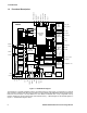
12: Peripheral Control Logic 12 PERIPHERAL CONTROL LOGIC (PCL) 12.1 Introduction The Peripheral Control Logic (PCL) is used to control GP4020 chip-wide functions. The PCL can be considered to have the following discrete functions: 1) Chip Reset logic 2) PLL Enable logic 3) Multiplex logic 4) Interrupt and wake-up logic 5) Chip status monitoring. 6) Chip-wide power-control 7) Test mode set-up Figure 12.1 below shows a block diagram of most of the functions that the PCL performs.
114 UIM BUS BSIO GPIO[0:7] GPIO[0:7] MULTIPLEX LOGIC GPIO[0:7] RF_PLL_LOCK IP_READ REGISTER UIM ADDRESS & DATA BUS EXT_NCS0 PER_INT BSIO_MUX[1:0] DISCOP_MUX IO_REV REGISTER MFNIO_CFG[2:0] POW_CNTL REGISTER CLR_SLEEP POWER_GOOD POWG_EN DISCIO_CFG[2:0] DISCOP DISCIO_READ POWER_GOOD TIMEMARK TIC MULTI_FNIO_READ MAG0 SIGN0 TESTMODE CHIP_REV [5:0] RF_PD GPIO[0:7] NSLP_RESET UART_CLK UIM_TEST MFNIO_CFG[2:0] RF_SLEEP MULTI_FNIO_READ DISCIO_READ DISCIO_CFG[2:0] BSIO_MUX[1:0] DISC
12: Peripheral Control Logic MULTI_FNIO D Q EXT_NCS0 NPOR_ RESET Q D WATCH_TM WAT_RESET 1 NSRESET NSRST_RESET RTC_CLK POWER_GOOD POW_RESET PLL_RESET 1 1 D D Q Q EN_POW_RST Q RF_PLL_LOCK UART_CLK 1 D EN_PLL_RST SFT_RESET PLL_IN_SEL[1:0] LATCH PLL_PD PLL_SLEEP 2 BIT UP=3 COUNTER = 3 BIT UP- =7 COUNTER INT_NCS0 NPOR_RESET A software Reset signal, SFT_RESET, can be set to initiate a reset of the Firefly MF1 and the 12-channel correlator by writing a '0' to bit 4 of the PER_S
12: Peripheral Control Logic RF_PLL_LOCK NRESET 3 CYCLES UART_CLK Any Freq Figure 12.3 RF_PLL_LOCK Hardware Reset Generation POWER_GOOD NRESET 3 CYCLES UART_CLK Any Freq Figure 12.4 POWER_GOOD Hardware Reset Generation when POWG_EN = '0', and UART_CLK NOT derived from an RF Front-end. POWER DOWN MODE 5ms POWER_GOOD RF_PLL_LOCK NRESET 3 CYCLES - 150ns UART_CLK Any Freq CLKI / CLKT UNDEFINED 20MHz Figure 12.5 POWER_GOOD Hardware Reset Generation when POWG_EN = '1'.
12: Peripheral Control Logic NSRESET NPOR_RESET NRESET RTC_CLK 3 CYCLES - 150ns UART_CLK Any Freq 20MHz RTC_CLK period = 30517ns. Rising edge only shown. Figure 12.6 NSRESET Hardware Reset Generation WATCH_TM NPOR_RESET NRESET RTC_CLK 3 CYCLES - 150ns UART_CLK Any Freq 20MHz RTC_CLK period = 30517ns. Rising edge only shown. Figure 12.7 Watchdog Hardware Reset Generation 1 CYCLE SFT_RESET NRESET 3 CYCLES UART_CLK Any Freq Figure 12.
12: Peripheral Control Logic either WATCH_TM or NSRESET signals. Therefore, a complete GP4020 reset can only occur if an NSRESET or a WATCH_TM event is introduced. These are synchronised to the 32kHz clock developed by the Real Time Clock, and the resulting output is active low. Additionally, the Reset status bits in PER_STAT[4:0] will only be reset by an asynchronous NSRESET event or a set of the CLR_RST bit to '0' in PER_STAT register, and will NOT be cleared by any other reset.
12: Peripheral Control Logic PLL_PD / PLL_SLEEP PLL_IN_SEL value change ....................... OR ........................ ....................... OR ........................ NRESET <30.5us 6 RTC_CLK cycles = 183us PLL_ENABLE RTC_CLK Figure 12.9 PLL_ENABLE Timing The selection of an external ROM in place of the Internal Boot ROM can also be determined during a reset.
12: Peripheral Control Logic SS[1] MULTI_FNIO_READ SS[0] BSIO DATA CLK CLK100KHz UART_CLK BSIO_MUX[1:0] MULTI_FNIO '0' '1' UIM_TEST MFNIO_CFG[2:0] SIGN1 DISCIO_READ MAG1 GPIO[0:7] RF_PD 0 0 1 1 2 2 TIC 3 3 '0' 4 4 5 5 6 6 7 7 RF_SLEEP GPIO[0:7] DISCIO '1' DISCIO_CFG[2:0] DISCIP1 DISCOP_MUX UIM_TEST DISCOP PLLDT1 Figure 12.10 Peripheral Control Logic - Multiplex Logic DISCIO_CFG[2:0] DISCIO Function 0xx Input only; read using DISCIO bit in IP_READ register.
12: Peripheral Control Logic GPIO output line number Alternative signal multiplex 0 BSIOCLK SIGN 1 Not available in standard operation Condition BSIO_MUX[1:0] = '10', '01', '11' UIM_TEST = '1' (i.e. TEST = High TESTMODE = High) 1 BSIODATA MAG 1 Not available in standard operation BSIO_MUX[1:0] = '10', '01', '11' UIM_TEST = '1' (i.e.
12: Peripheral Control Logic A single Interrupt line, PER_INT, is produced from 3 Peripheral Control Logic Interrupt signals from the Real Time Clock (RTC_CMP_INT), the 1PPS Timemark Generator (TIC_INT), and the POWER_GOOD input (Pin 64 (100-pin package)). The PER_INT interrupt is connected to the Firefly Interrupt Controller, and the signal which generated PER_INT interrupt can be determined from the RTC_CMP_INT, POW_GD_INT and TIC_INT bits of the PER_STAT register.
12: Peripheral Control Logic Note: the WATCH_EN bit in only effects Watchdog behaviour due to Firefly reset. (If WATCH_EN is set to '1', the Watchdog starts immediately. If WATCH_EN is '0', Watchdog will only start after the RESTART KEY value is written to it). h) Firefly and Correlator block reset, due to NRESET. This feature cannot be disabled. 12.6 Chip-wide Power Control modes The GP4020 incorporates a number of disable and power-saving modes. 12.6.
12: Peripheral Control Logic 12.6.2 RF Input and RF Front-end Power-Down A Power-down of an RF Front-end IC, along with disabling the 40MHz Low Level Differential Input cell in the System Clock Generator, can be made to occur if: a) RF_PD bit (POW_CNTL[0]) set to '1'. b) RF_SLEEP bit (POW_CNTL[10]) set to '1'. Under these conditions, the following pins on the GP4020 (100-pin package) get set as follows: • • Set as High Impedance (i.e.
12: Peripheral Control Logic Address Offset Register Direction Function Function Block 0x000 RTC_PRE Read Real Time Clock Pre-scaler value RTC 0x002 RTC_SEC_B Read 16 LSBs of Real Time Clock second counter RTC 0x004 COMP_RTCP Read /Write Comparison value for Real Time Clock Pre-scaler RTC 0x006 COMPS_RTCS Read /Write Comparison value for 8 LSBs of Real Time Clock Second counter, and 8 MSBs of Real Time Clock second counter RTC 0x008 POW_CNTL Read /Write Power Control Register PC
12: Peripheral Control Logic Bit No. 10 Mnemonic RF_SLEEP Description '1' = Disable 40MHz low-level differential input in System Clock Generator, and apply an active High power-down signal to the RF Front-end (via DISCIO (pin 55 (100-pin package)), if so configured (ref. IO_REV register). Can be re-enabled by a wake-up event.
12: Peripheral Control Logic Note: For each change of value of PLL_IN_SEL[1:0] or at PLL wake-up, the PLL will be disabled for a wait period of approx. 183µs (6 * 32kHz clock cycles, determined by the Real Time Clock block). This allows the CLKINB to stabilise. 12.7.
12: Peripheral Control Logic 12.7.3 PCL Input Read register - IP_READ - Memory Offset 0x00E This Read-only register allows the most recent state of a number of GP4020 input signals to be read. Bit No. Mnemonic Description Reset Value R/W 15 PER_INT PER_INT interrupt line, sourced by Peripheral Control Logic to Firefly MF1 core.
12: Peripheral Control Logic Bit No. 13 Mnemonic POW_INT_EN Description Enable PER_INT Interrupt signal to Interrupt Controller in Firefly MF1, due to POW_GD_INT (POWER_GOOD (pin 64) going Low.) Reset Value R/W 0 R/W 0 R/W 1 R/W 0 R/W 0 R 0 R 1 R/W 1 R/W 1 R/W R/W '1' = Enable Interrupt due to POWER_GOOD Low '0' = Disable 12 RCMP_INT_EN Enable PER_INT Interrupt signal to Interrupt Controller in Firefly MF1, due to RTC_CMP_INT signal from Real Time Clock.
12: Peripheral Control Logic Bit No. 2 Mnemonic POW_RESET (See Note 2) Description '1' = Reset due to POWER_GOOD = Low, has occurred since last CLR_RST or NSRESET clear-event. Reset Value R/W 0 R 0 R 0 R ‘0’ = No reset event due to POWER_GOOD has occurred 1 WAT_RESET (See Note 2) '1' = Reset due to Watchdog Time-out, has occurred since last CLR_RST or NSRESET clear-event.
13: Real Time Clock 13 REAL TIME CLOCK (RTC) 13.1 Introduction The Real Time Clock (RTC) is used to provide an incremental time indicator. It is based on a 32768Hz watchcrystal oscillator, with a 15-bit divider to produce a 1Hz clock, and a 24-bit counter accumulator to count seconds from zero upto a maximum of 194days (approx. 6 months). The RTC operates on the principle of incremental elapsed seconds, rather than absolute time.
13: Real Time Clock crystal need to be set to ensure that the total loop gain of the oscillator is high enough to guarantee continuous oscillation under all conditions. Normally this will mean that a loop gain of greater than 1 is needed. A set of equations for calculating C1 and C2 are explained in Section 14.3 "Processor Crystal Oscillator" on page 137. In the case of this 32.768kHz oscillator, key parameters are:Transconductance (gm) = 9.
13: Real Time Clock Bit No. Mnemonic Description 15:1 RTC_PRE[15:1] Reset Value Number of RTC clock cycles at sample time, within 1 second since last divider reset/rollover. (One clock cycle = 1/32768 = 30.5µs). R/W 0x0000 R 0 R/W Most Significant Bit = Bit 15. Note: This data ONLY reset by writing ‘0’ to bit 0 of this register. NOT resettable by any other reset source. 0 RTC_RESB Write '0': Reset RTC Counter and divider Write '1': No effect Read: Always read '0' Table 13.
13: Real Time Clock Bit No. 15:8 Mnemonic RTC_SEC_T[7:0] Description 8 MSBs of accumulated RTC seconds since last 24-bit counter reset. Reset Value R/W 0x00 R 0xFF R/W Most Significant Bit = Bit 15 Note: This data ONLY reset by writing ‘0’ to bit 0 of RTC_PRE. NOT resettable by any other reset source. 7:0 COMP_RTCS[7:0] 8-bit RTC Counter Comparison Value. Most Significant Bit = Bit 7. Table 13.
14: System Clock Generator 14 SYSTEM CLOCK GENERATOR (SCG) 14.1 Introduction The System Clock Generator (SCG) is used to generate two clock signals for the GP4020: • • The UART_CLK which runs UART2 continuously and produces the BµILD Clock. The BµILD Clock runs all the BµILD bus components, including the Firefly MF1 core with the ARM7TDMI microprocessor via a disable gate in the Peripheral Control Logic Block. The Correlator Master Clock (M_CLK).
14: System Clock Generator 14.2 40MHz Low Level Differential Input The 40MHz low-level differential input can process the 40MHz signal from a RF Front-end chip. The signal should have a DC bias of less than approx. 1.7V with respect to GND, and the 40MHz signal should have amplitude of approx. 100mV at a frequency of 40MHz. As a minimum, the CLK_I and CLK_T signals from the RF Front-end should be present in order to provide a phase-locked 40MHz M_CLK clock signal to the 12-channel correlator block.
14: System Clock Generator 14.3 Processor Crystal Oscillator The Processor Crystal Oscillator may need to be used with an external crystal, to generate the clock source for the UART_CLK signal.
14: System Clock Generator Zo = Output Impedance of oscillator at PRX_OUT Gm = Transconductance of oscillator Rf = Feedback Resistor (on-chip) ESR = Equivalent Series Resistance of crystal F = Fundamental Crystal frequency Equations 1 and 2 above can be used to calculate the range of tolerable crystal capacitance values, when the crystal characteristics are known (frequency and ESR). Typical values for C1 and C2 for a 10.0MHz crystal will be 47pF each, and for a 16.0MHz crystal will be 39pF each.
14: System Clock Generator Vcc Vdd (NOT Vcc) 33 1M 100nF 1nF IC1 PRX_IN Vcc 10uF 100nF TCXO 100 47nF GP4020 10.0MHz PRX_OUT 3.3V p-p GND 1V p-p ~1k 47nF ~0.5V p-p To RF Front-end PLL Ref input IC1 = ANY 3.3V High-speed CMOS Inverter. Figure 14.4 Connections of a TCXO frequency reference to the GP4020 Processor Crystal Oscillator 14.4 Phase Locked Loop (PLL) 14.4.1 Features • • • • • • Output clock frequencies from 10MHz to 250MHz Phase alignment offset: 0.
14: System Clock Generator Figure 14.5 GP4020 System Clock Generator PLL Configuration The PLL can provide accurate phase alignment between a generated clock and a reference clock without incurring delays normally associated with buffering. The PLL will phase lock the output clock ‘CLKOUTB’ to the referenceinput clock 'CLKINB'.
14: System Clock Generator PIN DESCRIPTION VCOD[1:0] PLL VCO Output Frequency Range selection pin. This input determines which of the 4 frequency ranges are selected. '00' operates the VCO between 80MHz and 250MHz; '01' operates the VCO between 40MHz and 125MHz; '10' operates the VCO between 20MHz and 63MHz; '11' operates the VCO between 10MHz and 32MHz PD PLL power down and reset pin. When PD is high the PLL is powered down, the ‘CLKOUTB’ output is forced high and all cells within the PLL are reset.
14: System Clock Generator If you intend to change the frequency of the PLL on the fly during time-critical code-execution, care should be used to ensure that the PLL is allowed to stabilise before allowing the code execution to continue. It is recommended that the software waits for the period specified by the “Worst-case settling time” parameter in Table 14.2 on page 142, Table 14.3 on page 143 and Table 14.4 on page 144 after the new frequency has been programmed in.
14: System Clock Generator UART _CLK O/P Freq. (MHz) I/P Freq.
14: System Clock Generator UART_CLK O/P Freq. (MHz) POW_CNTL register value PLL_CNTL register value 10.0 0x803C 0x197F Comments PLL bypassed and disabled PLL_CNTL value = reset value 11.25 0x80D8 0x018E 12.5 0x8098 0x09C6 13.75 0x80D8 0x01D2 15.0 0x8058 0x1202 16.25 0x80D8 0x0256 17.5 0x8098 0x0A4A 18.75 0x80D8 0x029A 20.0 0x8036 0x197F PLL bypassed and disabled PLL_CNTL value = reset value 21.25 0x80D8 0x02DE 22.5 0x8098 0x018E 23.75 0x80D8 0x0362 0x09C6 25.
14: System Clock Generator PLL Mult Factor Desired PLL output frequency Prog. Divider Control DIV[4:0] PLL SYNC MODE SYNCEN Charge Pump setting CHP[4:0] VCO Freq. Range Worst case settling time. VCOD[1:0] (µs) 8 40-125MHz 00110 0 9 40-125MHz 00111 0 01011 01 38 01100 01 10 40-125MHz 01000 36 0 01101 01 35 11 40-125MHz 12 40-125MHz 01001 0 01111 01 32 01010 0 10000 01 31 Table 14.5 PLL configuration options with input freq.
14: System Clock Generator 5) Output frequency of PLL; the higher the output frequency, the more current consumed: i. 240MHz = 6.2mA; ii. 125MHz = 4.5mA; iii. 60MHz = 3.4mA; iv. 30MHz = 2.9mA As a general rule of thumb, the lower the PLL input frequency, the lower the PLL output frequency and the lower the UART_CLK divider ratio, the lower the power-consumption of the SCG. 14.
14: System Clock Generator Bit No. 7:6 Mnemonic B_CLK_SEL[1:0] Description UART_CLK divider block selector. Reset Value R/W 00 R/W 1 R/W 10 R/W 1 R/W 1 R/W 0 R/W Allows selection of different output division ratios for the UART_CLK signal, to allow small resolution changes in UART_CLK frequency, if required. The divider ratio is set to divide by 1, in the reset condition. 5 PLL_BYP ‘00’ = divide by 1 (i.e.
14: System Clock Generator 14.6.2 SCG PLL Control Register - PLL_CNTL - Memory Offset 0x00A A write to this register stores logic values which set or reset input control lines to the PLL within the System Clock Generator. A read of this register shows the status of these functions. Bit No.
15: 1PPS Timemark Generator 15 1PPS TIMEMARK GENERATOR 15.1 Introduction The One Pulse Per Second (1PPS) Timemark Generator is nominally used to provide a 1 ms pulse, once every second, which is phase-aligned to Universal Time Co-ordinated (UTC), in conjunction with GPS system software. The Navstar GPS system relies absolutely on accurate timing information using Atomic clocks in the GPS Satellites.
150 UIM BUS M_CLK (from SYSTEM CLOCK GENERATOR) UIM BUS NPOR_RESET (FROM PCL) UIM ADDRESS & DATA BUS UIM BUS NOTE: TIC_RET[15:8] is NOT RESET by NPOR_RESET TIM_DEL[15:0] TIM_DEL[21:16] TIM_DEL_ENAB TIMEMARK _CONTROL[6:0] PROG_TIC _LOW[15:0] PROG_TIC _HIGH[4:0] PER_STAT [15:14] TIC_RET[15:0] 5.
15: 1PPS Timemark Generator 0.0999999s 10 TIC Periods = 0.999999s TIC ARM_TIMEMARK RAW TIMEMARK Figure 15.2 Timemark output using ARM_TIMEMARK signal, triggered from software. The TIC period can only be adjusted in steps of 175ns ( 7 / 40MHz = 175ns). Therefore, the closest that TIC can be set to 0.1000000s is either 0.0999999s or 0.100000075s.
15: 1PPS Timemark Generator SECONDS 0 1 2 1us delay 2us delay UTC TIC 10 TIC Periods = 0.999999s ARM_TIMEMARK RAW_TIMEMARK 1ms TIMEMARK 1ms TIMEMARK DELAY Figure 15.3 Typical timing relationship between UTC, TIC and Timemark, for small Timemark Delay values The GP4020 employs two separate sets of logic to allow the Timemark output to be aligned to UTC to a resolution of 25ns: 1) TIC period slewing – refer to Section 15.4 on page 155 2) Timemark Delay Counter – refer to Section 15.
15: 1PPS Timemark Generator iv) The value of the TIC period is at a given TIC. This can be calculated precisely with respect to UTC if the Receiver Clock Offset is known. v) The value of UTC at a given TIC, and hence the delay required to be added to a TIC occurrence, in order for Timemark to be aligned to TIC. vi) Delays due to the RF components and filters (i.e. Group-delay of SAW filters, etc.). These will generally dominate any static error in absolute timing of 1PPS.
15: 1PPS Timemark Generator TOTAL max. oscillator drift error = (a) + (b). In practice, the drift is much less than this under typical conditions ≈ 10 to 20ns 5. Computation induced error: It is assumed that enough significant bits are retained such that this error approximates zero. 6.
15: 1PPS Timemark Generator 15.4 Fine-resolution Timemark setting, using TIC period slewing 15.4.1 Functional description The GP4020 includes some logic within the 1PPS Timemark Generator which allows the TIC period to be specified to a resolution of 1 M_CLK cycle (25ns), without significantly affecting the existing logic in the correlator core. The default period of TIC is set to be 99999.9µs. Hence it will normally be necessary to add an extra 100ns to the effective period of TIC.
15: 1PPS Timemark Generator TIC_INT_EN[1:0] = '01'. Indicates that the TIC period will automatically be corrected independently of GPS software each time the phase_counter reaches 7, by means of the RELOAD_TIC signal. Each TIC event triggers a new phase_offset calculation. When the new phase_offset calculation is complete, TIC_INT is set (even if TIC period correction is not required). The ADJ_TIC_RD bit indicates if the next TIC period will be extended. Writing to ADJ_TIC has no effect.
15: 1PPS Timemark Generator TIC Event TIC_ CORR [2:0] Phase Offset Offset delay (ns) Over flow Next TIC Period (µs) Cumulated Overflow Overflow delay (ns) Total Delay (ns) 0 100 0 0 0 99999.9 0 0 0 1 100 4 100 0 99999.9 0 0 100 2 100 1 25 1 100000.075 1 175 200 3 100 5 125 0 99999.9 1 175 300 4 100 2 50 1 100000.075 2 350 400 5 100 6 150 0 99999.9 2 350 500 6 100 3 75 1 100000.075 3 525 600 7 100 0 0 1 100000.
15: 1PPS Timemark Generator 15.4.5 Timemark setting example 3 - TIC period Slewing with +2.5ppm Receiver Clock Offset For TIC period errors which are larger than +0.75ppm due to an offset in the Receiver clock, it will be necessary for the receiver to adjust the TIC period to be longer, using the PROG_TIC_HIGH and PROG_TIC_LOW registers. For example, if the receiver clock offset is noted to be +2.
15: 1PPS Timemark Generator TIC Event TIC_ CORR [2:0] Phase Offset Offset delay (ns) Over flow Next TIC Period (µs) Cumulated Overflow Overflow delay (ns) Total Delay (ns) 5 001 5 125 0 99999.975 0 0 125 6 001 6 150 0 99999.975 0 0 150 7 001 0 0 1 100000.150 1 175 175 8 001 1 25 0 99999.975 1 175 200 9 001 2 50 0 99999.975 1 175 225 10 001 3 75 0 99999.975 1 175 250 Table 15.
15: 1PPS Timemark Generator 6) The Timemark delay counter will continue counting down to 0, at which point the TIMEMARK output register will be cleared and the counter will stop. 7) At the next Timemark event, the same delay value will be used in the Timemark delay counter, unless a new value has been programmed in. The value of TIM_DEL_LO MUST be set before programming the TIM_DEL_HI register.
15: 1PPS Timemark Generator 15.5.3 Timemark setting example 6 - Timemark Delay Counter with +0.5ppm Receiver Clock Offset In practice, the TIC period could be upto ±2.5ppm in error due to the Receiver Clock Offset (drift in the receiver TCXO), which equates to approx. ±250ns in a TIC period of 0.0999999s. When a GPS receiver has acquired four or more satellite signals, and has achieved a first fix, the receiver should be able to deduce the error in TIC period due to Receiver Clock offset.
15: 1PPS Timemark Generator Timemark Event (s) TIC Event TIC Time (s) Required delay (µs) TIM_DEL value TIM_DEL _LO TIM_DEL_ HI 0 1 2 3 0 10 20 30 0 0.9999965 1.999993 2.9999895 0 3.5 7 10.5 40000 40140 40280 40420 0x9C40 0x9CCC 0x9D58 0x9DE4 0x40 0x40 0x40 0x40 100 101 1000 1010 99.999650 100.9996465 350 353.5 54000 54140 0xD2F0 0xD37C 0x40 0x40 182 183 1820 1830 181.999363 182.9993595 637 640.5 65480 65620 0xFFC8 0x0054 0x40 0x41 1000 1001 10000 10010 999.996500 1000.
15: 1PPS Timemark Generator Timemark Event (s) TIC Event TIC Time (s) Required delay (µs) TIM_DEL value TIM_DEL _LO TIM_DEL _HI 0 0 (TIC ADD) 0 0 40000 0x9C40 0x40 1 9 0.90000135 99998.65 4039946 0xA50A 0x7D 2 19 1.90000285 99997.15 4039886 0xA4CE 0x7D 3 29 2.90000435 99995.65 4039826 0xA492 0x7D 100 999 99.90014985 99850.15 4034006 0x8DD6 0x7D 101 1009 100.90015135 99848.65 4033946 0x8D99 0x7D 1000 9999 999.9014999 98500.
15: 1PPS Timemark Generator 15.7 1PPS Timemark Generator Registers The Timemark Generator uses four registers. These registers are addressable in the same part of the memory map as the Peripheral Control Logic Block - Root address 0x4010 1000. Address Offset Register Direction Function 0x010 PER_STAT Read/Write Used to set interrupts and Resets for the WHOLE GP4020 chip. Primarily used in the Peripheral Control Logic (PCL) block.
15: 1PPS Timemark Generator 15.7.2 1PPS Timemark Generator TIC Retention Register- TIC_RET - Memory Offset 0x012 This register combines control and monitor lines for the 1PPS Timemark Generator TIC period slewing logic, with an 8-bit data retention register. Note: Bit No. 15:8 The Data Retention register bits in the TIC_RET register are NOT reset by any reset event. This can only be cleared by writing ‘0x00’ or powering off GP4020. Mnemonic RETEN[7:0] Description Data Retention Register.
15: 1PPS Timemark Generator 15.7.4 1PPS Timemark Generator Delay Counter Register (MSB) - TIM_DEL_HI - Memory Offset 0x016 This register sets the six most significant bits for the 22-bit Timemark Delay Counter down-count initialised value, TIM_DEL, in conjunction with TIM_DEL_LO (see above). This is primarily a write-only register, but on reading the register, the settings made by the previous Write can be observed. Bit No.
16: Up-Integration Module 16 UP-INTEGRATION MODULE (UIM) The GP4020 contains the Firefly MF1 core, within which is a Memory Peripheral Controller (MPC) which contains a module called the Up Integration Module (UIM).
16: Up-Integration Module This Page intentionally left blank.
17: UARTs 17 UNIVERSAL ASYNCHRONOUS RECEIVER TRANSMITTER (UART) 17.1 Introduction The GP4020 uses two Universal Asynchronous Receiver Transmitter (UART) modules, which are components that provide industry-standard levels of support for full-duplex asynchronous serial communications, with appropriate mechanisms for software flow control. Neither UART1 nor UART2 support flow control with modem handshake signals (RTS, CTS, DTR, and DSR).
17: UARTs Whilst these are the same frequency, the BµILD_CLK can be disabled by using the F_SLEEP facility (refer to Section 12.5 "Interrupt and Wake-up logic" on page 121, for more information). In both UARTs, the clock pre-scaler, 16 bits long, is configured to generate a reference clock of period ‘Sclk divided by 1, 2, 4, 8, 16, 32, 64, 128, …. upto 32768’, as specified by one of the 16 combinations of value [0000 to 1111] programmed into the UART Division Select (MR[7:4]) register.
17: UARTs Baud Rate Required Division Select Value Reference Clock (MHz) Baud Rate Ratio Prog. BRR Value Programmed Baud Rate Baud Rate Error (%) 1200 8 2.65625 137.34635 137 1203.012 -0.251 2400 4 5.3125 137.34635 137 2406.024 -0.251 4800 2 10.625 137.34635 137 4812.047 -0.251 9600 1 21.25 137.34635 137 9624.094 -0.251 19200 1 21.25 68.173177 68 19248.19 -0.251 38400 1 21.25 33.586589 34 37946.43 1.181 57600 1 21.25 22.057726 22 57744.57 -0.
17: UARTs Baud Rate Required Division Select Value Reference Clock (MHz) Baud Rate Ratio Prog. BRR Value Programmed Baud Rate Baud Rate Error (%) 1200 8 3.125 161.76042 162 1198.236 0.147 2400 4 6.25 161.76042 162 2396.472 0.147 4800 2 12.5 161.76042 162 4792.945 0.147 9600 1 25 161.76042 162 9585.89 0.147 19200 1 25 80.380208 80 19290.12 -0.469 38400 1 25 39.690104 40 38109.76 0.756 57600 1 25 26.126736 26 57870.37 -0.469 76800 1 25 19.
17: UARTs Baud Rate Required Division Select Value Reference Clock (MHz) Baud Rate Ratio Prog. BRR Value Programmed Baud Rate Baud Rate Error (%) 1200 8 3.59375 186.17448 186 1201.12 -0.093 2400 4 7.1875 186.17448 186 2402.239 -0.093 4800 2 14.375 186.17448 186 4804.479 -0.093 9600 1 28.75 186.17448 186 9608.957 -0.093 19200 1 28.75 92.58724 93 19115.69 0.439 38400 1 28.75 45.79362 46 38231.38 0.439 57600 1 28.75 30.195747 30 57963.71 -0.
17: UARTs Baud Rate Required Division Select Value Reference Clock (MHz) Baud Rate Ratio Prog. BRR Value Programmed Baud Rate Baud Rate Error (%) 1200 8 4.375 226.86458 227 1199.287 0.059 2400 4 8.75 226.86458 227 2398.575 0.059 4800 2 17.5 226.86458 227 4797.149 0.059 9600 1 35 226.86458 227 9594.298 0.059 19200 1 35 112.93229 113 19188.6 0.059 38400 1 35 55.966146 56 38377.19 0.059 57600 1 35 36.977431 37 57565.79 0.059 76800 1 35 27.
17: UARTs This Page intentionally left Blank GP4020 GPS Baseband Processor Design Manual 175
18: Watchdog Timer 18 WATCHDOG TIMER (WDOG) The function of the Watchdog Timer block [WDOG] is to detect hardware or run-time software errors. It performs this function by requiring the processor to write to one of its registers periodically. Should this not occur, the Watchdog will time-out and reset the system. This ensures that hardware/software lock-ups are recoverable. A ® watchdog timer exists on the BµILD bus to verify that the ARM code is always in a known state.
18: Watchdog Timer WATCH_EN START PRIMARY DOWN-COUNTER =0 32BIT WATCH_INT CLR START UART_CLK SECONDARY DOWN-COUNTER =0 8BIT DIV 16 WATCH_TM RELOAD BUILD BUS READ CONSTAT [11:0] [7:0] CLR TEST BUILD BUS INTERFACE RESTART = KEY 0XECD9F7BD Figure 18.1 Watchdog Block Diagram 18.2 Operational Description The watchdog consists of two counters; the primary, which is 32-bits long, and the secondary, which is 8-bits long.
18: Watchdog Timer To restart the watchdog counter, a specific 32-bit value (=0xECD9F7BD; the RESTART key) must be programmed into the watchdog restart register.
18: Watchdog Timer All Watchdog Registers are 32-bits wide. 18.3.1 Watchdog Control / Status Register - CONSTAT - Memory Offset 0x000 The control register is 32-bits wide, with unused bits defined as zero. Attempts to access the register as a byte or a half-word will cause a bus error exception. Bit No. Mnemonic 31:20 19 EN Description Reset Value R/W Reserved 0 - Mask that controls whether the zero count state of the watchdog generates an interrupt to the ARM7TDMI processor.
18: Watchdog Timer 18.3.4 Watchdog Restart Register - RESTART - Memory Offset 0x00C Bit No. 31: 0 Mnemonic RESTART _KEY Description Reset Value Restart Key. A write to this register with the correct key value, 0xECD9F7BD, restarts the WDOG primary counter. 0x00000000 R/W W Table 18.5 Watchdog RESTART Register 18.3.5 Watchdog TEST Register - TEST - Memory Offset 0x010 This register is only accessible when the GP4020 is put into TEST mode (i.e.
19: System Address Map 19 ADDRESS MAPS 19.1 GP4020 System Address Map The GP4020 has the Address Map as shown in Table 19.1 below. ADDRESS RANGE FUNCTION 0x0000 0000 - 0x000F FFFF Internal Boot ROM or External Boot ROM via NSCS[0] 0x0010 0000 - 0x1FFF FFFF Not Used (Int./Ext.
19: System Address Map a) Gate NSCS[2A] externally with SADD[19] to produce a smaller external address space for NSCS[2A], but without the reflection of the internal logic once every 0x2000. The truth-table shown in Table 19.2 below: NSCS[2A] SADD[19] EXTERNAL CHIP SELECT 0 1 0 (ENABLED) 0 0 1 (DISABLED) 1 1 1 (DISABLED) 1 0 1 (DISABLED) Table 19.
19: System Address Map 19.2 GP4020 Firefly MF1 Address Map The Firefly MF1 BµILD bus modules have the address map as shown in Table 19.6 below, in the range 0xE000 0000 to 0xE007 FFFF.
19: System Address Map This page intentionally left blank.
20: Input / Output pin Characteristics 20 INPUT / OUTPUT PIN CHARACTERISTICS The GP4020 Electrical Characteristics, which are specific to the GP4020 device are shown in the “GP4020 GPS Baseband Processor Datasheet”, DS5134, available from Zarlink Semiconductor. In this section, the generic characteristics of the Input Output pins, and some timing diagrams of important external interfaces are shown. The data shown here should be used in conjunction with the data in the datasheet specified above. 20.
20: Input / Output pin Characteristics Pin No. 186 Pin Name Pin Type IP / OP Cell Type 5V Tol.
20: Input / Output pin Characteristics Pin No. Pin Name Pin Type IP / OP Cell Type 5V Tol.
20: Input / Output pin Characteristics Input edge 0.1ns Switching Delay (ns) Input edge 1.5ns Load (fF) Load (fF) 50 100 250 500 1000 50 100 250 500 1000 IP → D ↑ 0.29 0.34 0.49 0.74 1.23 0.40 0.45 0.60 0.84 1.34 IP → D ↓ 0.29 0.31 0.39 0.51 0.76 0.62 0.64 0.72 0.84 1.09 Table 20.2 3.3V Input delays 20.2.2 5V Tolerant Inputs: SCJIO1NR01N, SCJIP1NR Switching characteristics at 25°C, 3.3V supply. Input edge 0.1ns Switching Delay (ns) Input edge 1.
20: Input / Output pin Characteristics 20.3.1.2 Normal N outputs (3.3V outputs): CLAIO1HD01N, CLAIO1NR01N, CLAOP01N. Input edge 0.1ns Switching Delay (ns) Input edge 1.5ns Load (pF) Load (pF) 10 20 40 80 150 10 20 40 80 150 D → OP ↑ 5.82 6.99 8.89 11.75 15.76 5.55 6.72 8.62 11.48 15.49 D → OP ↓ 5.55 6.75 8.60 11.18 14.48 6.37 7.56 9.42 11.99 15.30 T → OP ↑ 6.10 7.27 9.18 12.05 16.06 6.91 8.08 9.99 12.86 16.87 T → OP ↓ 5.49 6.66 8.49 11.04 14.33 6.30 7.
20: Input / Output pin Characteristics 20.3.2.2 Normal N outputs: CLAIO1HD03N, CLAOP03N. Input edge 0.1ns Switching Delay (ns) Input edge 1.5ns Load (pF) Load (pF) 10 20 40 80 150 10 20 40 80 150 D → OP ↑ 5.82 6.99 8.89 11.75 15.76 5.55 6.72 8.62 11.48 15.49 D → OP ↓ 5.55 6.75 8.60 11.18 14.48 6.37 7.56 9.42 11.99 15.30 T → OP ↑ 6.10 7.27 9.18 12.05 16.06 6.91 8.08 9.99 12.86 16.87 T → OP ↓ 5.49 6.66 8.49 11.04 14.33 6.30 7.47 9.30 11.85 15.
20: Input / Output pin Characteristics Parameter Cell Type Min Input Leakage All IP -1 Output (Tristate) Leakage All OP Typ Max Unit Conditions +1 µA No Pull Up/Down, VDD = 3.6V 1 µA No Pull Up/Down, VDD = 3.
20: Input / Output pin Characteristics This Page intentionally left blank.
21: Timing Characteristics 21 TIMING CHARACTERISTICS The timing parameters in this section assume a logic switching point of 50% of VDD: All inputs assume rise and fall times of nominally 2ns. Minimum (min) and maximum (max) figures are referenced at extremes of Voltage and Temperature. Important Notes: 1) All parameters will scale from their MIN to MAX value as temperature RISES or voltage FALLS. Their relationship, however, will always remain the same.
21: Timing Characteristics BuILD_CLK Taddr Taddrh Tncs Tncsh Tnoe Tnoeh SADDR NSCS NSWE NSOE Tdisu SDATA Tdih Figure 21.2 MPC Timing Diagram - External Memory Read Cycle Note: These MPC Write and Read transactions are the same whether the ARM7TDMI core or the DMA Controller is the current bus master. Parameter Min Max Unit Description and notes Tsclk 14.0 ns BµILD Clk low period Tsclkh 14.0 ns BµILD Clk high period Taddr 12.2 31.5 ns BµILD Clk to Address Valid Taddrh 10.7 28.
21: Timing Characteristics 21.2 Memory Peripheral Controller (MPC) External Read & Write timing parameters with SWait Control Memory accesses with SWait control have default of one wait-state access, in addition to additional wait-states triggered by an external SWait = High signal. Read Transaction Default wait state External wait state Completion cycle BuILD_CLK SADDR NSCS NSWE NSOE SDATA Twh SWAIT Twsu Figure 21.
21: Timing Characteristics For this example an edge triggered packet transfer (size = 2) is shown. NOTE: When performing a DMA transfer, memory signals are as per the MPC timing information. Parameter Min Max Unit Description and notes Tdreq 0 ns Dreq setup before BµILD_CLK Tdreq_hold 7.5 ns Dreq hold time after BµILD_CLK Tdack 14.2 29.8 ns BµILD_CLK to Dack active Tdackh 11.1 29.0 ns Dack hold after BµILD_CLK (Dack1 & Dack2) Table 21.
21: Timing Characteristics 21.6 System Services Module (SSM) Broadcast Diagnostic Timing Diagrams The SBDIAG lines referred to here are the Xdiag[3:0] lines which can be configured within the SSM to be multiplexed with the JTAG interface, to allow access to any SADD or SDATA line within the Firefly MF1. BuILD_CLK Tbgdo Tbgdoh SDATA Tbdiag Tbdiagh SBDIAG Figure 21.6 External Broadcast diagnostic signal (SBDIAG) timings from SSM. Parameter Typ. units Description and notes Tbgdo 10.
21: Timing Characteristics Parameter Min Max units Description and notes Tbscl 15.6 - ns TCK low period Tbsch 15.6 - ns TCK high period Tbsis 5.0 - ns TDI,TMS setup to [TCr] Tbsih 5.0 - ns TDI,TMS hold from [TCr] Tbsoh 2.4 - ns TDO hold time Tbsod - 25 ns TCr to TDO valid Tbsr 25 - ns Reset period Table 21.
INDEXES GP4020 GPS Baseband Processor Design Manual Index - I
This page intentionally left blank Index - II GP4020 GPS Baseband Processor Design Manual
Table of Figures Page Figure 1.1 GP4020 Block Diagram ......................................................................................................................2 Figure 1.2 Block Diagram of typical GP4020 based GPS receiver.........................................................................8 Figure 2.1 GP4020 100-pin package pin distribution........................................................................................... 11 Figure 2.2 GP4020 100-pin package outline drawing........
Figure 12.10 Peripheral Control Logic - Multiplex Logic .................................................................................... 120 Figure 12.11 Peripheral Control Logic - Peripheral Interrupt and Wake-up control logic ..................................... 121 Figure 13.1 Real Time Clock Block Diagram .................................................................................................... 131 Figure 14.1 System Clock Generator Block Diagram ..........................................
This page intentionally left blank GP4020 GPS Baseband Processor Design Manual Index - V
Table of Data Tables Page Table 2.1 GP4020 100-pin package dimensions ........................................................................13 Table 2.2 GP4020 100-pin package Signal Descriptions ............................................................16 Table 3.1 Standard 32-bit ARM instruction set ...........................................................................21 Table 3.2 16-bit Thumb instruction set .......................................................................................
Table 7.18 CORR CHx_CODE_DCO_PHASE Register .............................................................74 Table 7.19 CORR CHx_CODE_DCO_PRESET_PHASE Register ..............................................74 Table 7.20 CORR CHx_CODE_PHASE Register .......................................................................75 Table 7.21 CORR CHx_CODE_PHASE_COUNTER Register ....................................................75 Table 7.22 CORR CHx_CODE_SLEW_COUNTER Register ........................................
Table 12.8 PCL PER_STAT Register ......................................................................................130 Table 13.1 Real Time Clock Register Map ...............................................................................132 Table 13.2 RTC_PRE Register................................................................................................133 Table 13.3 RTC_SEC_B Register............................................................................................133 Table 13.
Table 18.1 Watchdog Register Map.........................................................................................178 Table 18.2 Watchdog CONSTAT Register ...............................................................................179 Table 18.3 Watchdog RELOAD Register .................................................................................179 Table 18.4 Watchdog READ Register ......................................................................................179 Table 18.
This page intentionally left blank Index - X GP4020 GPS Baseband Processor Design Manual
For more information about all Zarlink products visit our Web Site at www.zarlink.com Information relating to products and services furnished herein by Zarlink Semiconductor Inc. or its subsidiaries (collectively “Zarlink”) is believed to be reliable.