
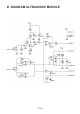
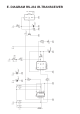
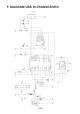
Instructions Circuit Diagram


- 114 -
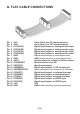
G. FLAT CABLE CONNECTIONS
Pin 1 SCL Serial Clock (for I2C communication)
Pin 2 SDA Serial Data (voor I2C communication)
Pin 3 PC3(ADC3) Digital input/output or analog monitor input
Pin 4 PC2(ADC2) Digital input/output or analog monitor input
Pin 5 PC1(ADC1) Digital input/output or analog monitor input
Pin 6 PC0(ADC0) Digital input/output or analog monitor input
Pin 7 GND GND (several connectors to prevent signal noise)
Pin 8 GND GND (several connectors to prevent signal noise)
Pin 9 AVCC Analog reference-voltage for AD-converters
Pin 10 PC6(RESET) Microcontroller reset pin
Pin 11 PB5(SCK) Digital input/output
Pin 12 PB4(MISO) Digital input/output or I2C function pin
Pin 13 PB3(MOSI/OC2) Digital input/output or I2C function pin or Timer2 pin
Pin 14 PD3(INT1) Digital input/output or external interrupt
Pin 15 PD6(AIN0) Digital input/output or analog testinput
Pin 16 D7(AIN1) Digital input/output or analog testinput
Pin 17 PD0(RXD) Digital input/output or RS232 input
Pin 18 PD1(TXD) Digital input/output or RS232 input
Pin 19 VCC VCC
Pin 20 GND GND (several connectors to prevent signal noise)