
Product Data Sheet

28
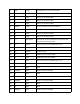
D10/PWM
Digital
GPIO; can be used as PWM
29
D11/MOSI
Digital
SPI MOSI; can be used as GPIO
30
D12/MISO
Digital
SPI MISO; can be used as GPIO
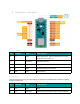
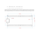
4.3 Debug
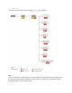
On the bottom side of the board, under the communication module, debug signals are arranged as 3x2
test pads with 100 mil pitch with pin 4 removed. Pin 1 is depicted in Figure 3 – Connector Positions
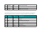
Pin
Function
Type
Description
1
+3V3
Power Out
Internally generated power output to be used as voltage
reference
2
SWD
Digital
nRF52480 Single Wire Debug Data
3
SWCLK
Digital In
nRF52480 Single Wire Debug Clock
5
GND
Power
Power Ground
6
RST
Digital In
Active low reset input