
Data Sheet
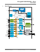
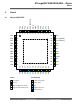

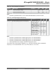
Table Of Contents
- Introduction
- Features
- Table of Contents
- 1. Block Diagram
- 2. Pinout
- 3. I/O Multiplexing and Considerations
- 4. Electrical Characteristics
- 4.1. Disclaimer
- 4.2. Absolute Maximum Ratings
- 4.3. General Operating Ratings
- 4.4. Power Considerations
- 4.5. Power Consumption
- 4.6. Peripherals Power Consumption
- 4.7. BOD and POR Characteristics
- 4.8. External Reset Characteristics
- 4.9. Oscillators and Clocks
- 4.10. I/O Pin Characteristics
- 4.11. USART
- 4.12. SPI
- 4.13. TWI
- 4.14. VREF
- 4.15. ADC
- 4.16. AC
- 4.17. UPDI Timing
- 4.18. Programming Time
- 5. Typical Characteristics
- 6. Ordering Information
- 7. Online Package Drawings
- 8. Package Drawings
- 9. Conventions
- 10. Data Sheet Revision History
- The Microchip Web Site
- Customer Change Notification Service
- Customer Support
- Product Identification System
- Microchip Devices Code Protection Feature
- Legal Notice
- Trademarks
- Quality Management System Certified by DNV
- Worldwide Sales and Service

4. Electrical Characteristics
4.1 Disclaimer
All typical values are measured at T = 25°C and V
DD
= 3V unless otherwise specified. All minimum and
maximum values are valid across operating temperature and voltage unless otherwise specified.
Typical values given should be considered for design guidance only, and actual part variation around
these values is expected.
4.2 Absolute Maximum Ratings
Stresses beyond those listed in this section may cause permanent damage to the device. This is a stress
rating only and functional operation of the device at these or other conditions beyond those indicated in
the operational sections of this specification is not implied. Exposure to absolute maximum rating
conditions for extended periods may affect device reliability.
Table 4-1. Absolute Maximum Ratings
Symbol Description Conditions Min. Max. Unit
V
DD
Power Supply Voltage -0.5 6 V
I
VDD
Current into a V
DD
pin T
A
=[-40, 85]°C - 200 mA
T
A
=[85, 125]°C - 100 mA
I
GND
Current out of a GND pin T
A
=[-40, 85]°C - 200 mA
T
A
=[85, 125]°C - 100 mA
V
PIN
Pin voltage with respect to GND -0.5 V
DD
+0.5 V
I
PIN
I/O pin sink/source current -40 40 mA
I
c1
(1)
I/O pin injection current except for the RESET pin V
pin
<GND-0.6V or
5.5V<V
pin
≤6.1V
4.9V<V
DD
≤5.5V
-1 1 mA
I
c2
(1)
I/O pin injection current except for the RESET pin V
pin
<GND-0.6V or
V
pin
≤5.5V
V
DD
≤4.9V
-15 15 mA
T
storage
Storage temperature -65 150 °C
Note:
1. – If V
PIN
is lower than GND-0.6V, then a current limiting resistor is required. The negative DC
injection current limiting resistor is calculated as R = (GND-0.6V – V
pin
)/I
Cn
.
– If V
PIN
is greater than V
DD
+0.6V, then a current limiting resistor is required. The positive DC
injection current limiting resistor is calculated as R = (V
pin
-(V
DD
+0.6))/I
Cn
.
4.3 General Operating Ratings
The device must operate within the ratings listed in this section in order for all other electrical
characteristics and typical characteristics of the device to be valid.
ATmega809/1609/3209/4809 – 48-pin
Electrical Characteristics
© 2019 Microchip Technology Inc.
Datasheet Preliminary
DS40002016B-page 9