
Data Sheet
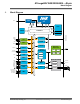
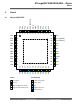

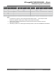
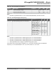
Table Of Contents
- Introduction
- Features
- Table of Contents
- 1. Block Diagram
- 2. Pinout
- 3. I/O Multiplexing and Considerations
- 4. Electrical Characteristics
- 4.1. Disclaimer
- 4.2. Absolute Maximum Ratings
- 4.3. General Operating Ratings
- 4.4. Power Considerations
- 4.5. Power Consumption
- 4.6. Peripherals Power Consumption
- 4.7. BOD and POR Characteristics
- 4.8. External Reset Characteristics
- 4.9. Oscillators and Clocks
- 4.10. I/O Pin Characteristics
- 4.11. USART
- 4.12. SPI
- 4.13. TWI
- 4.14. VREF
- 4.15. ADC
- 4.16. AC
- 4.17. UPDI Timing
- 4.18. Programming Time
- 5. Typical Characteristics
- 6. Ordering Information
- 7. Online Package Drawings
- 8. Package Drawings
- 9. Conventions
- 10. Data Sheet Revision History
- The Microchip Web Site
- Customer Change Notification Service
- Customer Support
- Product Identification System
- Microchip Devices Code Protection Feature
- Legal Notice
- Trademarks
- Quality Management System Certified by DNV
- Worldwide Sales and Service

...........continued
UQFN48/
TQFP48
Pin name
(1,2)
Special ADC0 AC0 USARTn SPI0 TWI0 TCA0 TCBn EVSYS CCL-LUTn
38 PF4 AIN14 2,TxD
(3)
0-WO4
(3)
0-WO
(3)
39 PF5 AIN15 2,RxD
(3)
0-WO5
(3)
1-WO
(3)
40 PF6 RESET 2,XCK
(3)
3-OUT
(3)
41 UPDI
42 VDD
43 GND
Note:
1. Pin names are of type Pxn, with x being the PORT instance (A,B,C, ...) and n the pin number.
Notation for signals is PORTx_PINn. All pins can be used as event input.
2. All pins can be used for external interrupt, where pins Px2 and Px6 of each port have full
asynchronous detection.
3. Alternate pin positions. For selecting the alternate positions, refer to the PORTMUX documentation.
ATmega809/1609/3209/4809 – 48-pin
I/O Multiplexing and Considerations
© 2019 Microchip Technology Inc.
Datasheet Preliminary
DS40002016B-page 8