
Data Sheet
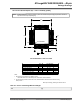
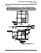
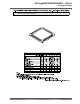
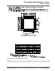

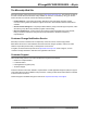
Table Of Contents
- Introduction
- Features
- Table of Contents
- 1. Block Diagram
- 2. Pinout
- 3. I/O Multiplexing and Considerations
- 4. Electrical Characteristics
- 4.1. Disclaimer
- 4.2. Absolute Maximum Ratings
- 4.3. General Operating Ratings
- 4.4. Power Considerations
- 4.5. Power Consumption
- 4.6. Peripherals Power Consumption
- 4.7. BOD and POR Characteristics
- 4.8. External Reset Characteristics
- 4.9. Oscillators and Clocks
- 4.10. I/O Pin Characteristics
- 4.11. USART
- 4.12. SPI
- 4.13. TWI
- 4.14. VREF
- 4.15. ADC
- 4.16. AC
- 4.17. UPDI Timing
- 4.18. Programming Time
- 5. Typical Characteristics
- 6. Ordering Information
- 7. Online Package Drawings
- 8. Package Drawings
- 9. Conventions
- 10. Data Sheet Revision History
- The Microchip Web Site
- Customer Change Notification Service
- Customer Support
- Product Identification System
- Microchip Devices Code Protection Feature
- Legal Notice
- Trademarks
- Quality Management System Certified by DNV
- Worldwide Sales and Service

RECOMMENDED LAND PATTERN
Dimension Limits
Units
C2Contact Pad Spacing
Contact Pitch
MILLIMETERS
0.50 BSC
MIN
E
MAX
8.40
Contact Pad Length (X48)
Contact Pad Width (X48)
Y1
X1
1.50
0.30
Microchip Technology Drawing C04-2300-PT Rev A
NOM
48-Lead Thin Quad Flatpack (PT) - 7x7x1.0 mm Body [TQFP]
C1
C2
E
X1
Y1
G
C1Contact Pad Spacing 8.40
Distance Between Pads G 0.20
BSC: Basic Dimension. Theoretically exact value shown without tolerances.
Notes:
Dimensioning and tolerancing per ASME Y14.5M
For best soldering results, thermal vias, if used, should be filled or tented to avoid solder loss during
reflow process
1.
2.
For the most current package drawings, please see the Microchip Packaging Specification located at
http://www.microchip.com/packaging
Note:
SILK SCREEN
1 2
48
Table 8-1. Device and Package Maximum Weight
140 mg
ATmega809/1609/3209/4809 – 48-pin
Package Drawings
© 2019 Microchip Technology Inc.
Datasheet Preliminary
DS40002016B-page 71