
Data Sheet
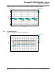
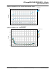
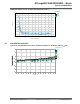
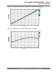
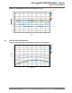
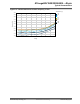
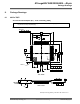
Table Of Contents
- Introduction
- Features
- Table of Contents
- 1. Block Diagram
- 2. Pinout
- 3. I/O Multiplexing and Considerations
- 4. Electrical Characteristics
- 4.1. Disclaimer
- 4.2. Absolute Maximum Ratings
- 4.3. General Operating Ratings
- 4.4. Power Considerations
- 4.5. Power Consumption
- 4.6. Peripherals Power Consumption
- 4.7. BOD and POR Characteristics
- 4.8. External Reset Characteristics
- 4.9. Oscillators and Clocks
- 4.10. I/O Pin Characteristics
- 4.11. USART
- 4.12. SPI
- 4.13. TWI
- 4.14. VREF
- 4.15. ADC
- 4.16. AC
- 4.17. UPDI Timing
- 4.18. Programming Time
- 5. Typical Characteristics
- 6. Ordering Information
- 7. Online Package Drawings
- 8. Package Drawings
- 9. Conventions
- 10. Data Sheet Revision History
- The Microchip Web Site
- Customer Change Notification Service
- Customer Support
- Product Identification System
- Microchip Devices Code Protection Feature
- Legal Notice
- Trademarks
- Quality Management System Certified by DNV
- Worldwide Sales and Service

Microchip Technology Drawing C04-300-PT Rev A Sheet 2 of 2
For the most current package drawings, please see the Microchip Packaging Specification located at
http://www.microchip.com/packaging
Note:
48-Lead Thin Quad Flatpack (PT) - 7x7x1.0 mm Body [TQFP]
H
L
(L1)
c
SECTION A-A
2.
1.
4.
BSC: Basic Dimension. Theoretically exact value shown without tolerances.
REF: Reference Dimension, usually without tolerance, for information purposes only.
3.
protrusions shall not exceed 0.25mm per side.
Mold Draft Angle Bottom
Molded Package Thickness
Dimension Limits
Mold Draft Angle Top
Note s :
Foot Length
Lead Width
Lead Thickness
Molded Package Length
Molded Package Width
Overall Length
Overall Width
Foot Angle
Footprint
Standoff
Overall Height
Lead Pitch
Number of Leads
12°
11° 13°
0.750.600.45L
12°
0.22
7.00 BSC
7.00 BSC
9.00 BSC
9.00 BSC
3.5°
1.00 REF
c
b
D1
E1
0.09
0.17
11°
D
E
L1
0°
13°
0.27
0.16-
7°
1.00
0.50 BSC
48
NOM
MILLIMETERS
A1
A2
A
e
0.05
0.95
-
Units
N
MIN
1.05
0.15
1.20
-
-
MAX
Chamfers at corners are optional; size may vary.
Pin 1 visual index feature may vary, but must be located within the hatched area.
Dimensioning and tolerancing per ASME Y14.5M
Dimensions D1 and E1 do not include mold flash or protrusions. Mold flash or
5.
plastic body at datum plane H
Datums A-B and D to be determined at center line between leads where leads exit
ATmega809/1609/3209/4809 – 48-pin
Package Drawings
© 2019 Microchip Technology Inc.
Datasheet Preliminary
DS40002016B-page 70