
Data Sheet
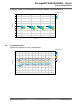
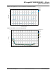
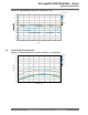
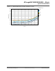
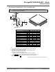
Table Of Contents
- Introduction
- Features
- Table of Contents
- 1. Block Diagram
- 2. Pinout
- 3. I/O Multiplexing and Considerations
- 4. Electrical Characteristics
- 4.1. Disclaimer
- 4.2. Absolute Maximum Ratings
- 4.3. General Operating Ratings
- 4.4. Power Considerations
- 4.5. Power Consumption
- 4.6. Peripherals Power Consumption
- 4.7. BOD and POR Characteristics
- 4.8. External Reset Characteristics
- 4.9. Oscillators and Clocks
- 4.10. I/O Pin Characteristics
- 4.11. USART
- 4.12. SPI
- 4.13. TWI
- 4.14. VREF
- 4.15. ADC
- 4.16. AC
- 4.17. UPDI Timing
- 4.18. Programming Time
- 5. Typical Characteristics
- 6. Ordering Information
- 7. Online Package Drawings
- 8. Package Drawings
- 9. Conventions
- 10. Data Sheet Revision History
- The Microchip Web Site
- Customer Change Notification Service
- Customer Support
- Product Identification System
- Microchip Devices Code Protection Feature
- Legal Notice
- Trademarks
- Quality Management System Certified by DNV
- Worldwide Sales and Service

Figure 5-61. Offset vs. V
REF
(V
DD
=5.0V, f
ADC
=115 ksps, REFSEL = External Reference)
-2.0
-1.6
-1.2
-0.8
-0.4
0.0
0.4
0.8
1.2
1.6
2.0
Offset [LSb]
1.8 2.6 4.096 4.3
Vref [V]
Temperature [°C]
-40
25
85
105
5.6 AC Characteristics
Figure 5-62. Hysteresis vs. V
CM
- 10 mV (V
DD
=5V)
0
2
4
6
8
10
12
14
16
18
20
Hysteresis [mV]
-0.5 0.0 0.5 1.0 1.5 2.0 2.5 3.0 3.5 4.0 4.5 5.0 5.5
Vcommon mode [V]
Temperature [°C]
-40
-20
0
25
55
85
105
125
ATmega809/1609/3209/4809 – 48-pin
Typical Characteristics
© 2019 Microchip Technology Inc.
Datasheet Preliminary
DS40002016B-page 61