
Data Sheet
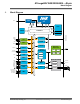
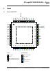

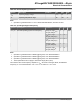
Table Of Contents
- Introduction
- Features
- Table of Contents
- 1. Block Diagram
- 2. Pinout
- 3. I/O Multiplexing and Considerations
- 4. Electrical Characteristics
- 4.1. Disclaimer
- 4.2. Absolute Maximum Ratings
- 4.3. General Operating Ratings
- 4.4. Power Considerations
- 4.5. Power Consumption
- 4.6. Peripherals Power Consumption
- 4.7. BOD and POR Characteristics
- 4.8. External Reset Characteristics
- 4.9. Oscillators and Clocks
- 4.10. I/O Pin Characteristics
- 4.11. USART
- 4.12. SPI
- 4.13. TWI
- 4.14. VREF
- 4.15. ADC
- 4.16. AC
- 4.17. UPDI Timing
- 4.18. Programming Time
- 5. Typical Characteristics
- 6. Ordering Information
- 7. Online Package Drawings
- 8. Package Drawings
- 9. Conventions
- 10. Data Sheet Revision History
- The Microchip Web Site
- Customer Change Notification Service
- Customer Support
- Product Identification System
- Microchip Devices Code Protection Feature
- Legal Notice
- Trademarks
- Quality Management System Certified by DNV
- Worldwide Sales and Service

2. Pinout
2.1 48-pin UQFN/TQFP
1
2
3
4
44
43
42
41
40
39
38
5
6
7
8
9
10
11
33
32
31
30
29
28
27
26
25
24
23
37
36
35
34
12
13
14
15
16
17
18
19
20
21
22
45
46
47
48
GND
VDD
PA5
PA6
PA7
PC0
PC1
PC4
PC5
PD2
PD3
PD6
PD7
PB0
PD0
PD1
PC3
PA2
PA3
PB1
PB2
PB3
PE1
PE2
PE0
PE3
PC2
GND
VDD
PF2
PF3
PF0 (TOSC1)
PF1 (TOSC2)
PF4
PD5
PC6
PC7
UPDI
PF5
PF6
PA1
PA4
PD4
PB4
PB5
GND
AVDD
PA0 (EXTCLK)
GPIO on VDD power domain
GPIO on AVDD power domain
Clock, crystal
Programming, debug
Input supply
Ground
TWI
Analog functions
Digital functions only
Power Functionality
ATmega809/1609/3209/4809 – 48-pin
Pinout
© 2019 Microchip Technology Inc.
Datasheet Preliminary
DS40002016B-page 6