
Data Sheet
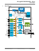
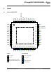

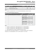
Table Of Contents
- Introduction
- Features
- Table of Contents
- 1. Block Diagram
- 2. Pinout
- 3. I/O Multiplexing and Considerations
- 4. Electrical Characteristics
- 4.1. Disclaimer
- 4.2. Absolute Maximum Ratings
- 4.3. General Operating Ratings
- 4.4. Power Considerations
- 4.5. Power Consumption
- 4.6. Peripherals Power Consumption
- 4.7. BOD and POR Characteristics
- 4.8. External Reset Characteristics
- 4.9. Oscillators and Clocks
- 4.10. I/O Pin Characteristics
- 4.11. USART
- 4.12. SPI
- 4.13. TWI
- 4.14. VREF
- 4.15. ADC
- 4.16. AC
- 4.17. UPDI Timing
- 4.18. Programming Time
- 5. Typical Characteristics
- 6. Ordering Information
- 7. Online Package Drawings
- 8. Package Drawings
- 9. Conventions
- 10. Data Sheet Revision History
- The Microchip Web Site
- Customer Change Notification Service
- Customer Support
- Product Identification System
- Microchip Devices Code Protection Feature
- Legal Notice
- Trademarks
- Quality Management System Certified by DNV
- Worldwide Sales and Service

1. Block Diagram
I
N
/
O
U
T
D
A
T
A
B
U
S
Clock Generation
BUS Matrix
CPU
USARTn
SPIn
TWIn
CCL
ACn
ADCn
TCAn
TCBn
WOn
RXD
TXD
XCK
XDIR
MISO
MOSI
SCK
SS
SDA (master)
SCL (master)
PORTS
EVSYS
System
Management
SLPCTRL
RSTCTRL
CLKCTRL
E
V
E
N
T
R
O
U
T
I
N
G
N
E
T
W
O
R
K
D
A
T
A
B
U
S
UPDI
CRC
SRAM
NVMCTRL
Flash
EEPROM
OSC20M
OSC32K
XOSC32K
References
BOD/
VLM
POR
Bandgap
WDT
RTC
CPUINT
M M
S
M
S
S
OCD
UPDI
RST
TOSC2
TOSC1
S
EXTCLK
LUTn-OUT
WO
CLKOUT
PAn
PBn
PCn
PDn
PEn
PFn
RESET
SDA (slave)
SCL (slave)
GPIOR
AINPn
AINNn
OUT
AINn
EVOUTx
VREFA
LUTn-INn
Detectors/
ATmega809/1609/3209/4809 – 48-pin
Block Diagram
© 2019 Microchip Technology Inc.
Datasheet Preliminary
DS40002016B-page 5