
Data Sheet
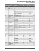
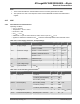

Table Of Contents
- Introduction
- Features
- Table of Contents
- 1. Block Diagram
- 2. Pinout
- 3. I/O Multiplexing and Considerations
- 4. Electrical Characteristics
- 4.1. Disclaimer
- 4.2. Absolute Maximum Ratings
- 4.3. General Operating Ratings
- 4.4. Power Considerations
- 4.5. Power Consumption
- 4.6. Peripherals Power Consumption
- 4.7. BOD and POR Characteristics
- 4.8. External Reset Characteristics
- 4.9. Oscillators and Clocks
- 4.10. I/O Pin Characteristics
- 4.11. USART
- 4.12. SPI
- 4.13. TWI
- 4.14. VREF
- 4.15. ADC
- 4.16. AC
- 4.17. UPDI Timing
- 4.18. Programming Time
- 5. Typical Characteristics
- 6. Ordering Information
- 7. Online Package Drawings
- 8. Package Drawings
- 9. Conventions
- 10. Data Sheet Revision History
- The Microchip Web Site
- Customer Change Notification Service
- Customer Support
- Product Identification System
- Microchip Devices Code Protection Feature
- Legal Notice
- Trademarks
- Quality Management System Certified by DNV
- Worldwide Sales and Service

...........continued
Symbol Description Conditions Min. Typ. Max. Unit
EABS Absolute
accuracy
REFSEL =
INTERNAL
V
REF
= 1.1V
T=[0-105]°C
V
DD
= [1.8V-3.6V]
- <10 - LSB
V
DD
= [1.8V-3.6V] - <15 -
REFSEL = V
DD
- 2.5 -
REFSEL =
INTERNAL
- <35 -
EGAIN Gain error REFSEL =
INTERNAL
V
REF
= 1.1V
T=[0-105]°C
V
DD
= [1.8V-3.6V]
- ±15 - LSB
V
DD
= [1.8V-3.6V] - ±20 -
REFSEL = V
DD
- 2 -
REFSEL =
INTERNAL
- ±35 -
EOFF Offset error REFSEL =
INTERNAL
V
REF
= 0.55V
- -1 - LSB
REFSEL =
INTERNAL
1.1V ≤ V
REF
- -0.5 - LSB
Note:
1. A DNL error of less than or equal to 1 LSB ensures a monotonic transfer function with no missing
codes.
2. These parameters are for design guidance only and are not production tested.
3. Reference setting and f
ADC
must fulfill the specification in “Clock and Timing Characteristics” and
“Power supply, Reference, and Input Range” tables.
4.15.2 External Reference Characteristics
Operating conditions:
• V
DD
= 1.8 to 5.5V
• Temperature = -40°C to 125°C
• DUTYCYC = 25%
• CLK
ADC
= 13 * f
ADC
• SAMPCAP is 5 pF
The accuracy characteristics numbers are based on the characterization of the following input reference
levels and V
DD
ranges:
• Vref = 1.8V, V
DD
= 1.8 to 5.5V
• Vref = 2.6V, V
DD
= 2.7 to 5.5V
• Vref = 4.096V, V
DD
= 4.5 to 5.5V
ATmega809/1609/3209/4809 – 48-pin
Electrical Characteristics
© 2019 Microchip Technology Inc.
Datasheet Preliminary
DS40002016B-page 27