
Data Sheet
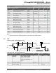
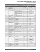
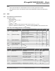
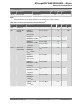

Table Of Contents
- Introduction
- Features
- Table of Contents
- 1. Block Diagram
- 2. Pinout
- 3. I/O Multiplexing and Considerations
- 4. Electrical Characteristics
- 4.1. Disclaimer
- 4.2. Absolute Maximum Ratings
- 4.3. General Operating Ratings
- 4.4. Power Considerations
- 4.5. Power Consumption
- 4.6. Peripherals Power Consumption
- 4.7. BOD and POR Characteristics
- 4.8. External Reset Characteristics
- 4.9. Oscillators and Clocks
- 4.10. I/O Pin Characteristics
- 4.11. USART
- 4.12. SPI
- 4.13. TWI
- 4.14. VREF
- 4.15. ADC
- 4.16. AC
- 4.17. UPDI Timing
- 4.18. Programming Time
- 5. Typical Characteristics
- 6. Ordering Information
- 7. Online Package Drawings
- 8. Package Drawings
- 9. Conventions
- 10. Data Sheet Revision History
- The Microchip Web Site
- Customer Change Notification Service
- Customer Support
- Product Identification System
- Microchip Devices Code Protection Feature
- Legal Notice
- Trademarks
- Quality Management System Certified by DNV
- Worldwide Sales and Service

Note:
1. These values are based on characterization and not covered by production test limits.
2. The symbols xxxx refer to the respective values of the AC0REFSEL bit field in the VREF.CTRLA
register.
4.15 ADC
4.15.1 Internal Reference Characteristics
Operating conditions:
• V
DD
= 1.8 to 5.5V
• Temperature = -40°C to 125°C
• DUTYCYC = 25%
• CLK
ADC
= 13 * f
ADC
• SAMPCAP is 10 pF for 0.55V reference, while it is set to 5 pF for V
REF
≥1.1V
• Applies for all allowed combinations of V
REF
selections and Sample Rates unless otherwise noted
Table 4-23. Power Supply, Reference, and Input Range
Symbol Description Conditions Min. Typ. Max. Unit
V
DD
Supply voltage CLK
ADC
≤1.5 MHz 1.8 - 5.5 V
CLK
ADC
>1.5 MHz 2.7 - 5.5
V
REF
Reference voltage REFSEL = Internal reference 0.55 - V
DD
-0.5 V
REFSEL = External reference 1.1 V
DD
REFSEL = V
DD
1.8 - 5.5
C
IN
Input capacitance SAMPCAP=5 pF - 5 - pF
SAMPCAP=10 pF - 10 -
V
IN
Input voltage range 0 - V
REF
V
I
BAND
Input bandwidth 1.1V≤V
REF
- - 57.5 kHz
Table 4-24. Clock and Timing Characteristics
(1)
Symbol Description Conditions Min. Typ. Max. Unit
f
ADC
Sample rate 1.1V≤V
REF
15 - 115 ksps
1.1V≤V
REF
(8-bit resolution) 15 - 150
V
REF
=0.55V (10 bits) 7.5 - 20
CLK
ADC
Clock frequency V
REF
=0.55V (10 bits) 100 - 260 kHz
1.1V≤V
REF
(10 bits) 200 - 1500
1.1V≤V
REF
(8-bit resolution) 200 - 2000
Ts Sampling time 2 2 33 CLK
ADC
cycles
T
CONV
Conversion time (latency) Sampling time = 2 CLK
ADC
8.7 - 50 µs
ATmega809/1609/3209/4809 – 48-pin
Electrical Characteristics
© 2019 Microchip Technology Inc.
Datasheet Preliminary
DS40002016B-page 25