
Data Sheet
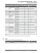
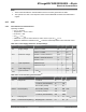
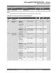
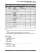

Table Of Contents
- Introduction
- Features
- Table of Contents
- 1. Block Diagram
- 2. Pinout
- 3. I/O Multiplexing and Considerations
- 4. Electrical Characteristics
- 4.1. Disclaimer
- 4.2. Absolute Maximum Ratings
- 4.3. General Operating Ratings
- 4.4. Power Considerations
- 4.5. Power Consumption
- 4.6. Peripherals Power Consumption
- 4.7. BOD and POR Characteristics
- 4.8. External Reset Characteristics
- 4.9. Oscillators and Clocks
- 4.10. I/O Pin Characteristics
- 4.11. USART
- 4.12. SPI
- 4.13. TWI
- 4.14. VREF
- 4.15. ADC
- 4.16. AC
- 4.17. UPDI Timing
- 4.18. Programming Time
- 5. Typical Characteristics
- 6. Ordering Information
- 7. Online Package Drawings
- 8. Package Drawings
- 9. Conventions
- 10. Data Sheet Revision History
- The Microchip Web Site
- Customer Change Notification Service
- Customer Support
- Product Identification System
- Microchip Devices Code Protection Feature
- Legal Notice
- Trademarks
- Quality Management System Certified by DNV
- Worldwide Sales and Service

...........continued
Symbol
(1)
Description Condition Min. Typ. Max. Unit
V
HYS
Hysteresis of
Schmitt trigger
inputs
0.1×V
DD
0.4×V
DD
V
V
OL
Output low voltage I
load
=20 mA, Fast mode+ - - 0.2xV
DD
V
I
load
=3 mA, Normal mode,
V
DD
>2V
- - 0.4V
I
load
=3 mA, Normal mode,
V
DD
≤2V
- - 0.2×V
DD
I
OL
Low-level output
current
f
SCL
≤400 kHz, V
OL
=0.4V 3 - - mA
f
SCL
≤1 MHz, V
OL
=0.4V 20 - -
C
B
Capacitive load for
each bus line
f
SCL
≤100 kHz - - 400 pF
f
SCL
≤400 kHz - - 400
f
SCL
≤1 MHz - - 550
t
R
Rise time for both
SDA and SCL
f
SCL
≤100 kHz - - 1000 ns
f
SCL
≤400 kHz 20 - 300
f
SCL
≤1 MHz - - 120
t
OF
Output fall time
from V
IHmin
to
V
ILmax
10 pF <
capacitance of
bus line < 400
pF
f
SCL
≤400
kHz
20+0.1×C
B
- 300 ns
f
SCL
≤1 MHz 20+0.1×C
B
- 120
t
SP
Spikes suppressed
by the input filter
0 - 50 ns
I
L
Input current for
each I/O pin
0.1×V
DD
<V
I
<0.9×V
DD
- - 1 µA
C
I
Capacitance for
each I/O pin
- - 10 pF
R
P
Value of pull-up
resistor
f
SCL
≤100 kHz (V
DD
-
V
OL
(max)) /I
OL
- 1000 ns/
(0.8473×C
B
)
Ω
f
SCL
≤400 kHz - - 300 ns/
(0.8473×C
B
)
f
SCL
≤1 MHz - - 120 ns/
(0.8473×C
B
)
t
HD;STA
Hold time
(repeated) Start
condition
f
SCL
≤100 kHz 4.0 - - µs
f
SCL
≤400 kHz 0.6 - -
f
SCL
≤1 MHz 0.26 - -
ATmega809/1609/3209/4809 – 48-pin
Electrical Characteristics
© 2019 Microchip Technology Inc.
Datasheet Preliminary
DS40002016B-page 22