
Data Sheet
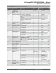
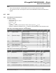
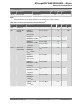

Table Of Contents
- Introduction
- Features
- Table of Contents
- 1. Block Diagram
- 2. Pinout
- 3. I/O Multiplexing and Considerations
- 4. Electrical Characteristics
- 4.1. Disclaimer
- 4.2. Absolute Maximum Ratings
- 4.3. General Operating Ratings
- 4.4. Power Considerations
- 4.5. Power Consumption
- 4.6. Peripherals Power Consumption
- 4.7. BOD and POR Characteristics
- 4.8. External Reset Characteristics
- 4.9. Oscillators and Clocks
- 4.10. I/O Pin Characteristics
- 4.11. USART
- 4.12. SPI
- 4.13. TWI
- 4.14. VREF
- 4.15. ADC
- 4.16. AC
- 4.17. UPDI Timing
- 4.18. Programming Time
- 5. Typical Characteristics
- 6. Ordering Information
- 7. Online Package Drawings
- 8. Package Drawings
- 9. Conventions
- 10. Data Sheet Revision History
- The Microchip Web Site
- Customer Change Notification Service
- Customer Support
- Product Identification System
- Microchip Devices Code Protection Feature
- Legal Notice
- Trademarks
- Quality Management System Certified by DNV
- Worldwide Sales and Service

...........continued
Symbol
(1)
Description Condition Min. Typ. Max. Unit
f
SSCK
Slave SCK clock frequency Slave - - 5 MHz
t
SSCK
Slave SCK period Slave 4*t Clkper - - ns
t
SSCKW
SCK high/low width Slave 2*t Clkper - - ns
t
SSCKR
SCK rise time Slave - - 1600 ns
t
SSCKF
SCK fall time Slave - - 1600 ns
t
SIS
MOSI setup to SCK Slave 3.0 - - ns
t
SIH
MOSI hold after SCK Slave t
Clkper
- - ns
t
SSS
SS setup to SCK Slave 21 - - ns
t
SSH
SS hold after SCK Slave 20 - - ns
t
SOS
MISO setup to SCK Slave - 8.0 - ns
t
SOH
MISO hold after SCK Slave - 13 - ns
t
SOSS
MISO setup after SS low Slave - 11 - ns
t
SOSH
MISO hold after SS low Slave - 8.0 - ns
Note:
1. These parameters are for design guidance only and are not production tested.
4.13 TWI
Figure 4-6. TWI - Timing Requirements
t
SU;STA
t
LOW
t
HIGH
t
LOW
t
of
t
HD;STA
t
HD;DAT
t
SU;DAT
t
SU;STO
t
BUF
SCL
SDA
t
r
Table 4-19. TWI - Timing Characteristics
Symbol
(1)
Description Condition Min. Typ. Max. Unit
f
SCL
SCL clock
frequency
Max. frequency requires
system clock at 10 MHz,
which, in turn, requires
V
DD
=[2.7, 5.5]V and T=[-40,
105]°C
0 - 1000 kHz
V
IH
Input high voltage 0.7×V
DD
- - V
V
IL
Input low voltage - - 0.3×V
DD
V
ATmega809/1609/3209/4809 – 48-pin
Electrical Characteristics
© 2019 Microchip Technology Inc.
Datasheet Preliminary
DS40002016B-page 21