
Data Sheet
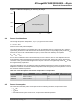
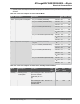

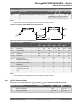
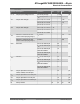
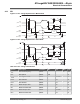
Table Of Contents
- Introduction
- Features
- Table of Contents
- 1. Block Diagram
- 2. Pinout
- 3. I/O Multiplexing and Considerations
- 4. Electrical Characteristics
- 4.1. Disclaimer
- 4.2. Absolute Maximum Ratings
- 4.3. General Operating Ratings
- 4.4. Power Considerations
- 4.5. Power Consumption
- 4.6. Peripherals Power Consumption
- 4.7. BOD and POR Characteristics
- 4.8. External Reset Characteristics
- 4.9. Oscillators and Clocks
- 4.10. I/O Pin Characteristics
- 4.11. USART
- 4.12. SPI
- 4.13. TWI
- 4.14. VREF
- 4.15. ADC
- 4.16. AC
- 4.17. UPDI Timing
- 4.18. Programming Time
- 5. Typical Characteristics
- 6. Ordering Information
- 7. Online Package Drawings
- 8. Package Drawings
- 9. Conventions
- 10. Data Sheet Revision History
- The Microchip Web Site
- Customer Change Notification Service
- Customer Support
- Product Identification System
- Microchip Devices Code Protection Feature
- Legal Notice
- Trademarks
- Quality Management System Certified by DNV
- Worldwide Sales and Service

Note:
1. Pin group A (PA[7:0]), PF[6:2]), pin group B (PB[7:0], PC[7:0]), pin group C (PD:7:0, PE[3:0],
PF[1:0]). For 28-pin and 32-pin devices pin group A and B should be seen as a single group. The
combined continuous sink/source current for each individual group should not exceed the limits.
2. These parameters are for design guidance only and are not production tested.
4.11 USART
Figure 4-3. USART in SPI Mode - Timing Requirements in Master Mode
MSb LSb
t
MOS
t
MIS
t
MIH
t
SCKW
t
SCK
t
MOH
t
MOH
t
SCKF
t
SCKR
t
SCKW
MOSI
(Data Output)
MISO
(Data Input)
SCK
(CPOL = 1)
SCK
(CPOL = 0)
SS
MSb LSb
Table 4-17. USART in SPI Master Mode - Timing Characteristics
Symbol
(1)
Description Condition Min. Typ. Max. Unit
f
SCK
SCK clock frequency Master - - 10 MHz
t
SCK
SCK period Master 100 - - ns
t
SCKW
SCK high/low width Master - 0.5×t
SCK
- ns
t
SCKR
SCK rise time Master - 2.7 - ns
t
SCKF
SCK fall time Master - 2.7 - ns
t
MIS
MISO setup to SCK Master - 10 - ns
t
MIH
MISO hold after SCK Master - 10 - ns
t
MOS
MOSI setup to SCK Master - 0.5×t
SCK
- ns
t
MOH
MOSI hold after SCK Master - 1.0 - ns
Note:
1. These parameters are for design guidance only and are not production tested.
ATmega809/1609/3209/4809 – 48-pin
Electrical Characteristics
© 2019 Microchip Technology Inc.
Datasheet Preliminary
DS40002016B-page 19