
Data Sheet
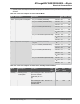
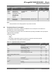
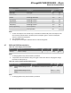

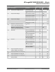
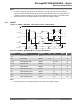
Table Of Contents
- Introduction
- Features
- Table of Contents
- 1. Block Diagram
- 2. Pinout
- 3. I/O Multiplexing and Considerations
- 4. Electrical Characteristics
- 4.1. Disclaimer
- 4.2. Absolute Maximum Ratings
- 4.3. General Operating Ratings
- 4.4. Power Considerations
- 4.5. Power Consumption
- 4.6. Peripherals Power Consumption
- 4.7. BOD and POR Characteristics
- 4.8. External Reset Characteristics
- 4.9. Oscillators and Clocks
- 4.10. I/O Pin Characteristics
- 4.11. USART
- 4.12. SPI
- 4.13. TWI
- 4.14. VREF
- 4.15. ADC
- 4.16. AC
- 4.17. UPDI Timing
- 4.18. Programming Time
- 5. Typical Characteristics
- 6. Ordering Information
- 7. Online Package Drawings
- 8. Package Drawings
- 9. Conventions
- 10. Data Sheet Revision History
- The Microchip Web Site
- Customer Change Notification Service
- Customer Support
- Product Identification System
- Microchip Devices Code Protection Feature
- Legal Notice
- Trademarks
- Quality Management System Certified by DNV
- Worldwide Sales and Service

Table 4-10. Brown-out Detector (BOD) Characteristics
Symbol Description Condition Min. Typ. Max. Unit
V
BOD
BOD detection level (falling/
rising)
BODLEVEL0 1.7 1.8 2.0 V
BODLEVEL2 2.4 2.6 2.9
BODLEVEL7 3.9 4.3 4.5
V
HYS
Hysteresis BODLEVEL0 - 25 - mV
BODLEVEL2 - 40 -
BODLEVEL7 - 80 -
t
BOD
Detection time Continuous - 7 - µs
Sampled, 1 kHz - 1 - ms
Sampled, 125 Hz - 8 -
t
startup
Start-up time Time from enable to ready - 40 - µs
V
INT
Interrupt level 0 Percentage above the selected
BOD level
- 4 - %
Interrupt level 1 - 13 -
Interrupt level 2 - 25 -
4.8 External Reset Characteristics
Table 4-11. External Reset Characteristics
Mode Description Condition Min. Typ. Max. Unit
V
VIH_RST
Input Voltage for RESET 0.7×V
DD
- V
DD
+0.2 V
V
VIL_RST
Input Low Voltage for RESET -0.2 - 0.3×V
DD
t
MIN_RST
Minimum pulse width on RESET pin
(1)
- - 2.5 µs
R
p_RST
RESET pull-up resistor V
Reset
=0V 20 35 50 kΩ
Note:
1. These parameters are for design guidance only and are not production tested.
4.9 Oscillators and Clocks
Operating conditions:
• V
DD
=3V, except where specified otherwise
Table 4-12. 20 MHz Internal Oscillator (OSC20M) Characteristics
Symbol Description Condition Min. Typ. Max. Unit
f
OSC20M
Factory calibration frequency FREQSEL=0 T
A
=25°C, 3.0V 16 MHz
FREQSEL=1 20
ATmega809/1609/3209/4809 – 48-pin
Electrical Characteristics
© 2019 Microchip Technology Inc.
Datasheet Preliminary
DS40002016B-page 15