
Data Sheet
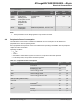

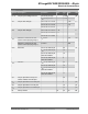
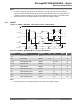
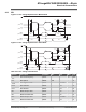
Table Of Contents
- Introduction
- Features
- Table of Contents
- 1. Block Diagram
- 2. Pinout
- 3. I/O Multiplexing and Considerations
- 4. Electrical Characteristics
- 4.1. Disclaimer
- 4.2. Absolute Maximum Ratings
- 4.3. General Operating Ratings
- 4.4. Power Considerations
- 4.5. Power Consumption
- 4.6. Peripherals Power Consumption
- 4.7. BOD and POR Characteristics
- 4.8. External Reset Characteristics
- 4.9. Oscillators and Clocks
- 4.10. I/O Pin Characteristics
- 4.11. USART
- 4.12. SPI
- 4.13. TWI
- 4.14. VREF
- 4.15. ADC
- 4.16. AC
- 4.17. UPDI Timing
- 4.18. Programming Time
- 5. Typical Characteristics
- 6. Ordering Information
- 7. Online Package Drawings
- 8. Package Drawings
- 9. Conventions
- 10. Data Sheet Revision History
- The Microchip Web Site
- Customer Change Notification Service
- Customer Support
- Product Identification System
- Microchip Devices Code Protection Feature
- Legal Notice
- Trademarks
- Quality Management System Certified by DNV
- Worldwide Sales and Service

Figure 4-1. Maximum Frequency vs. V
DD
for [-40, 105]°C
5MHz
10MHz
20MHz
1.8V 5.5V2.7V 4.5V
Safe Operating Area
4.4 Power Considerations
The average die junction temperature, T
J
(in °C) is given from the formula
T
J
= T
A
+P
D
* R
θJA
where P
D
is the total power dissipation.
The total thermal resistance of a package (R
θJA
) can be separated into two components, R
θJC
and R
θCA
,
representing the barrier to heat flow from the semiconductor junction to the package (case) surface (R
θJC
)
and from the case to the outside ambient air (R
θCA
). These terms are related by the equation:
R
θJA
= R
θJC
+ R
θCA
.
R
θJC
is device related and cannot be influenced by the user. However, R
θCA
is user dependent and can
be minimized by thermal management techniques such as heat sinks, ambient air cooling, and thermal
convection. Thus, good thermal management on the part of the user can significantly reduce R
θCA
so that
R
θJA
approximately equals R
θJC
.
The power dissipation curve is negatively sloped as ambient temperature increase. The maximum power
dissipation is therefore at minimum ambient temperature while the highest junction temperature occurs at
the maximum ambient temperature.
Table 4-4. Power Dissipation and Junction Temperature vs Temperature
Package T
A
Range R
θJA
(°C/W) P
D
(W) Typical T
J
- T
A
(°C) Typical
UQFN48 -40°C to 125°C 1.0
TQFP48 -40°C to 125°C 1.0
4.5 Power Consumption
The values are measured power consumption under the following conditions, except where noted:
• V
DD
=3V
• T
A
=25°C
• OSC20M used as system clock source, except where otherwise specified
ATmega809/1609/3209/4809 – 48-pin
Electrical Characteristics
© 2019 Microchip Technology Inc.
Datasheet Preliminary
DS40002016B-page 11