
Data Sheet
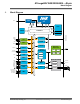
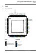

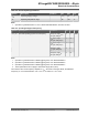
Table Of Contents
- Introduction
- Features
- Table of Contents
- 1. Block Diagram
- 2. Pinout
- 3. I/O Multiplexing and Considerations
- 4. Electrical Characteristics
- 4.1. Disclaimer
- 4.2. Absolute Maximum Ratings
- 4.3. General Operating Ratings
- 4.4. Power Considerations
- 4.5. Power Consumption
- 4.6. Peripherals Power Consumption
- 4.7. BOD and POR Characteristics
- 4.8. External Reset Characteristics
- 4.9. Oscillators and Clocks
- 4.10. I/O Pin Characteristics
- 4.11. USART
- 4.12. SPI
- 4.13. TWI
- 4.14. VREF
- 4.15. ADC
- 4.16. AC
- 4.17. UPDI Timing
- 4.18. Programming Time
- 5. Typical Characteristics
- 6. Ordering Information
- 7. Online Package Drawings
- 8. Package Drawings
- 9. Conventions
- 10. Data Sheet Revision History
- The Microchip Web Site
- Customer Change Notification Service
- Customer Support
- Product Identification System
- Microchip Devices Code Protection Feature
- Legal Notice
- Trademarks
- Quality Management System Certified by DNV
- Worldwide Sales and Service

Table 4-2. General Operating Conditions
Symbol Description Condition Min. Max. Unit
V
DD
Operating Supply Voltage 1.8
(1)
5.5 V
T
A
Operating temperature range -40 125 °C
Note:
1. Operation is guaranteed down to 1.8V or VBOD with BODLEVEL0, whichever is lower.
Table 4-3. Operating Voltage and Frequency
Symbol Description Condition Min. Max. Unit
f
CLK_CPU
Nominal operating system clock frequency V
DD
=[1.8, 5.5]V
T
A
=[-40, 105]°C
(1)(4)
0 5 MHz
V
DD
=[2.7, 5.5]V
T
A
=[-40, 105]°C
(2)(4)
0 10
V
DD
=[4.5, 5.5]V
T
A
=[-40, 105]°C
(3)(4)
0 20
V
DD
=[2.7, 5.5]V
T
A
=[-40, 125]°C
(2)
0 8
V
DD
=[4.5, 5.5]V
T
A
=[-40, 125]°C
(2)
0 16
Note:
1. Operation is guaranteed down to BOD triggering level, V
BOD
with BODLEVEL0.
2. Operation is guaranteed down to BOD triggering level, V
BOD
with BODLEVEL2.
3. Operation is guaranteed down to BOD triggering level, V
BOD
with BODLEVEL7.
4. These specifications do not apply to automotive range parts (-VAO).
The maximum CPU clock frequency depends on V
DD
. As shown in the figure below, the Maximum
Frequency vs. V
DD
is linear between 1.8V < V
DD
< 2.7V and 2.7V < V
DD
< 4.5V.
ATmega809/1609/3209/4809 – 48-pin
Electrical Characteristics
© 2019 Microchip Technology Inc.
Datasheet Preliminary
DS40002016B-page 10