ATmega809/1609/3209/4809 – 48-pin 48-pin Data Sheet – megaAVR® 0-series Introduction ® ® The ATmega809/1609/3209/4809 microcontrollers of the megaAVR 0-series are using the AVR processor with hardware multiplier, running at up to 20 MHz, with a wide range of Flash sizes up to 48 KB, up to 6 KB of SRAM, and 256 bytes of EEPROM in 28-, 32-, 40-, or 48-pin package.
ATmega809/1609/3209/4809 – 48-pin • • • • • – SleepWalking peripherals • Power-Down with limited wake-up functionality Peripherals – One 16-bit Timer/Counter type A (TCA) with a dedicated period register and three compare channels – Four 16-bit Timer/Counter type B with input capture (TCB) – One 16-bit Real-Time Counter (RTC) running from an external crystal or an internal RC oscillator – Four USART with fractional baud rate generator, auto-baud, and start-of-frame detection – Master/slave Serial Perip
ATmega809/1609/3209/4809 – 48-pin Table of Contents Introduction......................................................................................................................1 Features.......................................................................................................................... 1 1. Block Diagram........................................................................................................... 5 2. Pinout...........................................................
ATmega809/1609/3209/4809 – 48-pin 8. Package Drawings...................................................................................................69 8.1. 8.2. 48-Pin TQFP.............................................................................................................................. 69 48-Pin UQFN..............................................................................................................................73 9. Conventions..................................................
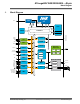
ATmega809/1609/3209/4809 – 48-pin Block Diagram 1.
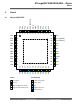
ATmega809/1609/3209/4809 – 48-pin Pinout PA3 PA2 PA1 PA0 (EXTCLK) GND VDD UPDI PF6 PF5 PF4 PF3 46 45 44 43 42 41 40 39 38 37 48-pin UQFN/TQFP 47 2.1 PA4 Pinout 48 2.
ATmega809/1609/3209/4809 – 48-pin I/O Multiplexing and Considerations 3. I/O Multiplexing and Considerations 3.
ATmega809/1609/3209/4809 – 48-pin I/O Multiplexing and Considerations ...........continued UQFN48/ TQFP48 Pin name (1,2) 38 PF4 AIN14 39 PF5 AIN15 40 PF6 41 UPDI 42 VDD 43 GND Special ADC0 RESET AC0 USARTn SPI0 TWI0 TCA0 TCBn 2,TxD(3) 0-WO4(3) 0-WO(3) 2,RxD(3) 0-WO5(3) 1-WO(3) 2,XCK(3) EVSYS CCL-LUTn 3-OUT(3) Note: 1. Pin names are of type Pxn, with x being the PORT instance (A,B,C, ...) and n the pin number. Notation for signals is PORTx_PINn.
ATmega809/1609/3209/4809 – 48-pin Electrical Characteristics 4. Electrical Characteristics 4.1 Disclaimer All typical values are measured at T = 25°C and VDD = 3V unless otherwise specified. All minimum and maximum values are valid across operating temperature and voltage unless otherwise specified. Typical values given should be considered for design guidance only, and actual part variation around these values is expected. 4.
ATmega809/1609/3209/4809 – 48-pin Electrical Characteristics Table 4-2. General Operating Conditions Symbol Description VDD TA Condition Min. Max. Unit Operating Supply Voltage 1.8(1) 5.5 V Operating temperature range -40 125 °C Note: 1. Operation is guaranteed down to 1.8V or VBOD with BODLEVEL0, whichever is lower. Table 4-3. Operating Voltage and Frequency Symbol Description Condition Min. Max. Unit fCLK_CPU Nominal operating system clock frequency VDD=[1.8, 5.
ATmega809/1609/3209/4809 – 48-pin Electrical Characteristics Figure 4-1. Maximum Frequency vs. VDD for [-40, 105]°C 20MHz 10MHz Safe Operating Area 5MHz 1.8V 4.4 2.7V 4.5V 5.5V Power Considerations The average die junction temperature, TJ (in °C) is given from the formula TJ = TA+PD * RθJA where PD is the total power dissipation.
ATmega809/1609/3209/4809 – 48-pin Electrical Characteristics • System power consumption measured with peripherals disabled and I/O ports driven low with inputs disabled Table 4-5. Power Consumption in Active and Idle Mode Mode Description Condition Typ. Max. Unit Active Active power consumption fCLK_CPU=20 MHz (OSC20M) VDD=5V 8.5 - mA fCLK_CPU=10 MHz (OSC20M div2) VDD=5V 4.3 - mA VDD=3V 2.3 - mA VDD=5V 2.2 - mA VDD=3V 1.2 - mA VDD=2V 0.75 - mA VDD=5V 16.4 - µA VDD=3V 9.
ATmega809/1609/3209/4809 – 48-pin Electrical Characteristics ...........continued Mode Description Condition Power Down/ Standby Power down/ All peripherals Standby power stopped consumption are the same when all peripherals are stopped Reset Reset power consumption Typ. 25°C VDD=3V 0.1 RESET line pulled low VDD=3V 100 Max. 85°C(1) Max. 125°C Unit 5.0 15.0 µA - - µA Note: 1. These parameters are for design guidance only and are not tested. 4.
ATmega809/1609/3209/4809 – 48-pin Electrical Characteristics ...........continued Peripheral Conditions Typ.(1) Unit XOSC32K CL=7.5 pF 0.5 µA 0.4 µA OSCULP32K USART Enable @ 9600 Baud 13.0 µA SPI (Master) Enable @ 100 kHz 2.1 µA TWI (Master) Enable @ 100 kHz 24.0 µA TWI (Slave) Enable @ 100 kHz 17.0 µA Flash programming Erase Operation 1.5 mA Write Operation 3.0 Note: 1. Current consumption of the module only.
ATmega809/1609/3209/4809 – 48-pin Electrical Characteristics Table 4-10. Brown-out Detector (BOD) Characteristics Symbol Description Condition Min. Typ. Max. Unit VBOD BODLEVEL0 1.7 1.8 2.0 BODLEVEL2 2.4 2.6 2.9 BODLEVEL7 3.9 4.3 4.
ATmega809/1609/3209/4809 – 48-pin Electrical Characteristics ...........continued Symbol Description Condition Min. Typ. Max. Unit fCAL Frequency calibration range OSC16M(2) 14.5 17.5 MHz OSC20M(2) 18.5 21.5 MHz -1.5 1.5 % TA=[0, 70]°C, -2.0 VDD=[1.8, 3.6]V 2.0 % Full operation range -4.0 4.0 TA=[0, 70]°C, -1.8 VDD=[1.8, 5.5]V 1.
ATmega809/1609/3209/4809 – 48-pin Electrical Characteristics ...........continued Symbol Description ESR(1) Equivalent Series Resistance - Safety Factor=3 Condition Min. Typ. Max. Unit CL=7.5 pF - - 80 CL=12.5 pF - - 40 kΩ Note: 1. This parameter is for design guidance only and not production tested. Figure 4-2. External Clock Waveform Characteristics V IH1 V IL1 Table 4-15. External Clock Characteristics Symbol Description Condition VDD=[1.8, 5.5]V VDD=[2.7, 5.5]V VDD=[4.5, 5.
ATmega809/1609/3209/4809 – 48-pin Electrical Characteristics ...........continued Symbol Description Condition Min. Typ. IIH / IIL VDD=5.5V, pin high - < 0.05 - VDD=5.5V, pin low - < 0.05 - VDD=1.8V, IOL=1.5 mA - - 0.36 VDD=3.0V, IOL=7.5 mA - - 0.6 VDD=5.0V, IOL=15 mA - - 1 VDD=1.8V, IOH=1.5 mA 1.44 - - VDD=3.0V, IOH=7.5 mA 2.4 - - VDD=5.
ATmega809/1609/3209/4809 – 48-pin Electrical Characteristics Note: 1. Pin group A (PA[7:0]), PF[6:2]), pin group B (PB[7:0], PC[7:0]), pin group C (PD:7:0, PE[3:0], PF[1:0]). For 28-pin and 32-pin devices pin group A and B should be seen as a single group. The combined continuous sink/source current for each individual group should not exceed the limits. 2. These parameters are for design guidance only and are not production tested. 4.11 USART Figure 4-3.
ATmega809/1609/3209/4809 – 48-pin Electrical Characteristics 4.12 SPI Figure 4-4. SPI - Timing Requirements in Master Mode SS tSCKR tMOS tSCKF SCK (CPOL = 0) tSCKW SCK (CPOL = 1) tSCKW tMIS MISO (Data Input) tMIH tSCK MSb LSb tMOH tMOH MOSI (Data Output) MSb LSb Figure 4-5. SPI - Timing Requirements in Slave Mode SS tSSCKR tSSS tSSCKF tSSH SCK (CPOL = 0) tSSCKW SCK (CPOL = 1) tSSCKW tSIS MOSI (Data Input) tSIH MSb tSOSS MISO (Data Output) tSSCK LSb tSOS tSOSH MSb LSb Table 4-18.
ATmega809/1609/3209/4809 – 48-pin Electrical Characteristics ...........continued Symbol(1) Description Condition Min. Typ. Max. Unit fSSCK Slave SCK clock frequency Slave - - 5 MHz tSSCK Slave SCK period Slave 4*t Clkper - - ns tSSCKW SCK high/low width Slave 2*t Clkper - - ns tSSCKR SCK rise time Slave - - 1600 ns tSSCKF SCK fall time Slave - - 1600 ns tSIS MOSI setup to SCK Slave 3.
ATmega809/1609/3209/4809 – 48-pin Electrical Characteristics ...........continued Symbol(1) Description Condition Min. VHYS Hysteresis of Schmitt trigger inputs 0.1×VDD VOL Output low voltage Iload=20 mA, Fast mode+ - Iload=3 mA, Normal mode, VDD>2V IOL CB tR tOF Low-level output current Output fall time from VIHmin to VILmax tSP Spikes suppressed by the input filter IL Input current for each I/O pin CI Capacitance for each I/O pin RP Value of pull-up resistor Unit 0.4×VDD V - 0.
ATmega809/1609/3209/4809 – 48-pin Electrical Characteristics ...........continued Symbol(1) Description tLOW Condition Min. Typ. Max. Unit 4.7 - - µs 1.3 - - 0.5 - - 4.0 - - 0.6 - - fSCL≤1 MHz 0.26 - - fSCL≤100 kHz 4.7 - - fSCL≤400 kHz 0.6 - - fSCL≤1 MHz 0.26 - - fSCL≤100 kHz 0 - 3.45 fSCL≤400 kHz 0 - 0.9 fSCL≤1 MHz 0 - 0.45 fSCL≤100 kHz 250 - - fSCL≤400 kHz 100 - - fSCL≤1 MHz 50 - - fSCL≤100 kHz 4 - - fSCL≤400 kHz 0.6 - - fSCL≤1 MHz 0.
ATmega809/1609/3209/4809 – 48-pin Electrical Characteristics ...........continued Symbol(1) Description Min. Typ. Max. Unit VDD Power supply voltage range for 0V55 1.8 - 5.5 V Power supply voltage range for 1V1 1.8 - 5.5 Power supply voltage range for 1V5 1.8 - 5.5 Power supply voltage range for 2V5 3.0 - 5.5 Power supply voltage range for 4V3 4.8 - 5.5 Note: 1. These parameters are for design guidance only and are not production tested. Table 4-21.
ATmega809/1609/3209/4809 – 48-pin Electrical Characteristics Note: 1. These values are based on characterization and not covered by production test limits. 2. The symbols xxxx refer to the respective values of the AC0REFSEL bit field in the VREF.CTRLA register. 4.15 ADC 4.15.1 Internal Reference Characteristics Operating conditions: • VDD = 1.8 to 5.5V • Temperature = -40°C to 125°C • DUTYCYC = 25% • CLKADC = 13 * fADC • SAMPCAP is 10 pF for 0.55V reference, while it is set to 5 pF for VREF≥1.
ATmega809/1609/3209/4809 – 48-pin Electrical Characteristics ...........continued Symbol Description Conditions Min. Typ. Max. Unit TSTART Internal VREF - Start-up time 22 - µs Note: 1. These parameters are for design guidance only and are not production tested. Table 4-25. Accuracy Characteristics Internal Reference(2) Symbol Description Res Resolution INL Integral Nonlinearity Conditions Min. Typ. Max. Unit - 10 - bit fADC=7.7 ksps - 1.
ATmega809/1609/3209/4809 – 48-pin Electrical Characteristics ...........continued Symbol Description Conditions EABS REFSEL = INTERNAL Absolute accuracy Min. Typ. Max. Unit - <10 - LSB - <15 - REFSEL = VDD - 2.5 - REFSEL = INTERNAL - <35 - - ±15 - - ±20 - REFSEL = VDD - 2 - REFSEL = INTERNAL - ±35 - REFSEL = INTERNAL - -1 - LSB - -0.5 - LSB VREF = 1.1V EGAIN Gain error REFSEL = INTERNAL VREF = 1.1V EOFF Offset error T=[0-105]°C VDD = [1.8V-3.6V] VDD = [1.
ATmega809/1609/3209/4809 – 48-pin Electrical Characteristics • Vref = 4.3V, VDD = 4.5 to 5.5V Table 4-26. ADC Accuracy Characteristics External Reference(2) Symbol Description Res Resolution INL Integral Nonlinearity DNL(1) EABS EGAIN EOFF Conditions Differential Non-linearity Absolute accuracy Gain error Min. Typ. Max. Unit - 10 - bit fADC=15 ksps - 0.9 - LSB fADC=77 ksps - 0.9 - fADC=115 ksps - 1.2 - fADC=15 ksps - 0.2 - fADC=77 ksps - 0.4 - fADC=115 ksps - 0.
ATmega809/1609/3209/4809 – 48-pin Electrical Characteristics ...........continued Symbol Description Condition Min. Typ. Max. Unit VHYS Hysteresis HYSMODE=0x0 - 0 - mV HYSMODE=0x1 - 10 - HYSMODE=0x2 - 25 - HYSMODE=0x3 - 50 - 25 mV Overdrive, VDD≥2.7V - 50 - ns Min. Typ. Max. Unit -0.2 - VDD V PD1 to PD6 - 3.5 - pF PD7 - 14 - 0.7V
ATmega809/1609/3209/4809 – 48-pin Electrical Characteristics 4.18 Programming Time See the table below for typical programming times for Flash and EEPROM. Table 4-29. Programming Times Symbol Typical Programming Time Page Buffer Clear 7 CLK_CPU cycles Page Write 2 ms Page Erase 2 ms Page Erase-Write 4 ms Chip Erase 4 ms EEPROM Erase 4 ms © 2019 Microchip Technology Inc.
ATmega809/1609/3209/4809 – 48-pin Typical Characteristics 5. Typical Characteristics 5.1 Power Consumption 5.1.1 Supply Currents in Active Mode Figure 5-1. Active Supply Current vs. Frequency (1-20 MHz) at T=25°C VDD [V] 12.0 1.8 2.2 2.7 3 3.6 4.2 5 5.5 11.0 10.0 9.0 8.0 7.0 6.0 5.0 4.0 3.0 2.0 1.0 0.0 0 2 4 6 8 10 12 14 16 18 20 Frequency [MHz] Figure 5-2. Active Supply Current vs. Frequency [0.1, 1.0] MHz at T=25°C VDD [V] 600 1.8 2.2 2.7 3 3.6 4.2 5 5.
ATmega809/1609/3209/4809 – 48-pin Typical Characteristics Figure 5-3. Active Supply Current vs. Temperature (f=20 MHz OSC20M) VDD [V] 12.0 4.5 5 5.5 11.0 10.0 9.0 8.0 7.0 6.0 5.0 4.0 3.0 2.0 1.0 0.0 -40 -20 0 20 40 60 80 100 120 Temperature [°C] Figure 5-4. Active Supply Current vs. VDD (f=[1.25, 20] MHz OSC20M) at T=25°C Frequency [MHz] 12.0 1.25 2.5 5 10 20 11.0 10.0 9.0 8.0 7.0 6.0 5.0 4.0 3.0 2.0 1.0 0.0 1.5 2.0 2.5 3.0 3.5 4.0 4.5 5.0 5.
ATmega809/1609/3209/4809 – 48-pin Typical Characteristics Figure 5-5. Active Supply Current vs. VDD (f=32.768 kHz OSCULP32K) Temperature [°C] 32 -40 -20 0 25 70 85 105 125 28 24 20 16 12 8 4 0 1.5 2.0 2.5 3.0 3.5 4.0 4.5 5.0 5.5 Vdd [V] 5.1.2 Supply Currents in Idle Mode Figure 5-6. Idle Supply Current vs. Frequency (1-20 MHz) at T=25°C VDD [V] 5.0 1.8 2.2 2.7 3 3.6 4.2 5 5.5 4.5 4.0 3.5 3.0 2.5 2.0 1.5 1.0 0.5 0.
ATmega809/1609/3209/4809 – 48-pin Typical Characteristics Figure 5-7. Idle Supply Current vs. Low Frequency (0.1-1.0 MHz) at T=25°C VDD [V] 250 1.8 2.2 2.7 3 3.6 4.2 5 5.5 225 200 175 150 125 100 75 50 25 0 0.0 0.1 0.2 0.3 0.4 0.5 0.6 0.7 0.8 0.9 1.0 Frequency [MHz] Figure 5-8. Idle Supply Current vs. Temperature (f=20 MHz OSC20M) VDD [V] 5.0 4.5 5 5.5 4.5 4.0 3.5 3.0 2.5 2.0 1.5 1.0 0.5 0.0 -40 -20 0 20 40 60 80 100 120 Temperature [°C] © 2019 Microchip Technology Inc.
ATmega809/1609/3209/4809 – 48-pin Typical Characteristics Figure 5-9. Idle Supply Current vs. VDD (f=32.768 kHz OSCULP32K) Temperature [°C] 20 -40 -20 0 25 70 85 105 125 18 16 14 12 10 8 6 4 2 0 1.5 2.0 2.5 3.0 3.5 4.0 4.5 5.0 5.5 Vdd [V] 5.1.3 Supply Currents in Power-Down Mode Figure 5-10. Power-Down Mode Supply Current vs. Temperature (all functions disabled) VDD [V] 8.0 1.8 2.2 2.7 3 3.6 4.2 5 5.5 7.0 6.0 5.0 4.0 3.0 2.0 1.0 0.
ATmega809/1609/3209/4809 – 48-pin Typical Characteristics Figure 5-11. Power-Down Mode Supply Current vs. VDD (all functions disabled) Temperature [°C] 8.0 -40 -20 0 25 70 85 105 125 7.0 6.0 5.0 4.0 3.0 2.0 1.0 0.0 1.5 2.0 2.5 3.0 3.5 4.0 4.5 5.0 5.5 Vdd [V] Figure 5-12. Power-Down Mode Supply Current vs. VDD (all functions disabled) Temperature [°C] 8.0 -40 -20 0 25 70 85 105 125 7.0 6.0 5.0 4.0 3.0 2.0 1.0 0.0 2.5 3.0 3.5 4.0 4.5 5.0 5.5 Vdd [V] © 2019 Microchip Technology Inc.
ATmega809/1609/3209/4809 – 48-pin Typical Characteristics 5.1.4 Supply Currents in Standby Mode Figure 5-13. Standby Mode Supply Current vs. VDD (RTC running with internal OSCULP32K) Temperature [°C] 10.0 -40 -20 0 25 70 85 105 125 9.0 8.0 7.0 6.0 5.0 4.0 3.0 2.0 1.0 0.0 1.5 2.0 2.5 3.0 3.5 4.0 4.5 5.0 5.5 Vdd [V] Figure 5-14. Standby Mode Supply Current vs. VDD (Sampled BOD running at 125 Hz) Temperature [°C] 10.0 -40 -20 0 25 70 85 105 125 9.0 8.0 7.0 6.0 5.0 4.0 3.0 2.0 1.0 0.0 1.5 2.
ATmega809/1609/3209/4809 – 48-pin Typical Characteristics Figure 5-15. Standby Mode Supply Current vs. VDD (Sampled BOD running at 1 kHz) Temperature [°C] 10.0 -40 -20 0 25 70 85 105 125 9.0 8.0 7.0 6.0 5.0 4.0 3.0 2.0 1.0 0.0 1.5 2.0 2.5 3.0 3.5 4.0 4.5 5.0 5.5 Vdd [V] 5.1.5 Power-on Supply Currents Figure 5-16. Power-on Supply Current vs. VDD (BOD enabled at 4.3V level) Temperature [°C] 400 -40 -20 0 25 70 85 105 125 360 320 280 240 200 160 120 80 40 0 0.0 0.5 1.0 1.5 2.0 2.5 3.
ATmega809/1609/3209/4809 – 48-pin Typical Characteristics GPIO GPIO Input Characteristics Figure 5-17. I/O Pin Input Hysteresis vs. VDD Temperature[°C] 2.0 -40 0 25 70 85 105 125 1.8 1.6 Threshold [V] 1.4 1.2 1.0 0.8 0.6 0.4 0.2 0.0 1.5 2.0 2.5 3.0 3.5 4.0 4.5 5.0 5.5 Vdd [V] Figure 5-18. I/O Pin Input Threshold Voltage vs. VDD (T=25°C) Treshold 75 Vih Vil 70 65 60 Threshold [%] 5.2 55 50 45 40 35 30 25 1.5 2.0 2.5 3.0 3.5 4.0 4.5 5.0 5.
ATmega809/1609/3209/4809 – 48-pin Typical Characteristics Figure 5-19. I/O Pin Input Threshold Voltage vs. VDD (VIH) Temperature[°C] 75 -40 0 25 70 85 105 125 70 65 Threshold [%] 60 55 50 45 40 35 30 25 1.5 2.0 2.5 3.0 3.5 4.0 4.5 5.0 5.5 Vdd [V] Figure 5-20. I/O Pin Input Threshold Voltage vs. VDD (VIL) Temperature[°C] 75 -40 0 25 70 85 105 125 70 65 Threshold [%] 60 55 50 45 40 35 30 25 1.5 2.0 2.5 3.0 3.5 4.0 4.5 5.0 5.5 Vdd [V] © 2019 Microchip Technology Inc.
ATmega809/1609/3209/4809 – 48-pin Typical Characteristics GPIO Output Characteristics Figure 5-21. I/O Pin Output Voltage vs. Sink Current (VDD=1.8V) Temperature[°C] 0.50 -40 -20 0 25 70 85 105 125 0.45 0.40 Voutput[V] 0.35 0.30 0.25 0.20 0.15 0.10 0.05 0.00 0.0 0.2 0.4 0.6 0.8 1.0 1.2 1.4 1.6 1.8 2.0 Sink current [mA] Figure 5-22. I/O Pin Output Voltage vs. Sink Current (VDD=3.0V) Temperature [°C] 0.50 -40 -20 0 25 70 85 105 125 0.45 0.40 0.35 0.30 0.25 0.20 0.15 0.10 0.05 0.
ATmega809/1609/3209/4809 – 48-pin Typical Characteristics Figure 5-23. I/O Pin Output Voltage vs. Sink Current (VDD=5.0V) Temperature [°C] 1.0 -40 -20 0 25 70 85 105 125 0.9 0.8 0.7 0.6 0.5 0.4 0.3 0.2 0.1 0.0 0 2 4 6 8 10 12 14 16 18 20 Sink current [mA] Figure 5-24. I/O Pin Output Voltage vs. Sink Current (T=25°C) Vdd [V] 1.0 1.8 2 2.2 3 4 5 0.9 0.8 Voutput[V] 0.7 0.6 0.5 0.4 0.3 0.2 0.1 0.0 0 2 4 6 8 10 12 14 16 18 20 Sink current [mA] © 2019 Microchip Technology Inc.
ATmega809/1609/3209/4809 – 48-pin Typical Characteristics Figure 5-25. I/O Pin Output Voltage vs. Source Current (VDD=1.8V) Temperature [°C] 1.80 -40 -20 0 25 70 85 105 125 1.75 1.70 1.65 1.60 1.55 1.50 1.45 1.40 1.35 1.30 0.0 0.2 0.4 0.6 0.8 1.0 1.2 1.4 1.6 1.8 2.0 Source current [mA] Figure 5-26. I/O Pin Output Voltage vs. Source Current (VDD=3.0V) Temperature [°C] 3.0 -40 -20 0 25 70 85 105 125 2.9 2.8 2.7 2.6 2.5 2.4 2.3 2.2 2.1 2.
ATmega809/1609/3209/4809 – 48-pin Typical Characteristics Figure 5-27. I/O Pin Output Voltage vs. Source Current (VDD=5.0V) Temperature [°C] 5.0 -40 -20 0 25 70 85 105 125 4.9 4.8 4.7 4.6 4.5 4.4 4.3 4.2 4.1 4.0 0 2 4 6 8 10 12 14 16 18 20 Source current [mA] Figure 5-28. I/O Pin Output Voltage vs. Source Current (T=25°C) Vdd [V] 5.0 1.8 2 2.2 3 4 5 4.5 4.0 Voutput[V] 3.5 3.0 2.5 2.0 1.5 1.0 0.5 0.
ATmega809/1609/3209/4809 – 48-pin Typical Characteristics GPIO Pull-Up Characteristics Figure 5-29. I/O Pin Pull-Up Resistor Current vs. Input Voltage (VDD=1.8V) Temperature [°C] 2.0 -40 -20 0 25 70 85 105 125 1.8 1.5 1.3 1.0 0.8 0.5 0.3 0.0 0 5 10 15 20 25 30 35 40 45 50 Pull-up resistor current [µA] Figure 5-30. I/O Pin Pull-Up Resistor Current vs. Input Voltage (VDD=3.0V) Temperature [°C] 3.0 -40 -20 0 25 70 85 105 125 2.8 2.5 2.3 2.0 1.8 1.5 1.3 1.
ATmega809/1609/3209/4809 – 48-pin Typical Characteristics Figure 5-31. I/O Pin Pull-Up Resistor Current vs. Input Voltage (VDD=5.0V) Temperature [°C] 5.0 -40 -20 0 25 70 85 105 125 4.8 4.5 4.3 4.0 3.8 3.5 3.3 3.0 0 5 10 15 20 25 30 35 40 45 50 Pull-up resistor current [µA] VREF Characteristics Figure 5-32. Internal 0.55V Reference vs. Temperature Vdd [V] 1.0 2 3 5 0.8 0.6 0.4 Vref error [%] 5.3 0.2 0.0 -0.2 -0.4 -0.6 -0.8 -1.
ATmega809/1609/3209/4809 – 48-pin Typical Characteristics Figure 5-33. Internal 1.1V Reference vs. Temperature Vdd [V] 1.0 2 3 5 0.8 0.6 Vref error [%] 0.4 0.2 0.0 -0.2 -0.4 -0.6 -0.8 -1.0 -40 -20 0 20 40 60 80 100 120 Temperature [°C] Figure 5-34. Internal 2.5V Reference vs. Temperature Vdd [V] 1.0 3 5 0.8 0.6 Vref error [%] 0.4 0.2 0.0 -0.2 -0.4 -0.6 -0.8 -1.0 -40 -20 0 20 40 60 80 100 120 Temperature [°C] © 2019 Microchip Technology Inc.
ATmega809/1609/3209/4809 – 48-pin Typical Characteristics Figure 5-35. Internal 4.3V Reference vs. Temperature Vdd [V] 1.0 5 0.8 0.6 Vref error [%] 0.4 0.2 0.0 -0.2 -0.4 -0.6 -0.8 -1.0 -40 -20 0 20 40 60 80 100 120 Temperature [°C] BOD Characteristics BOD Current vs. VDD Figure 5-36. BOD Current vs. VDD (Continuous Mode Enabled) Temperature [°C] 50 -40 0 25 70 85 105 125 45 40 35 30 Idd [µA] 5.4 25 20 15 10 5 0 1.5 2.0 2.5 3.0 3.5 4.0 4.5 5.0 5.
ATmega809/1609/3209/4809 – 48-pin Typical Characteristics Figure 5-37. BOD Current vs. VDD (Sampled BOD at 125 Hz) Temperature [°C] 5.0 -40 0 25 70 85 105 125 4.5 4.0 3.5 Idd [µA] 3.0 2.5 2.0 1.5 1.0 0.5 0.0 1.5 2.0 2.5 3.0 3.5 4.0 4.5 5.0 5.5 Vdd [V] Figure 5-38. BOD Current vs. VDD (Sampled BOD at 1 kHz) Temperature [°C] 5.0 -40 0 25 70 85 105 125 4.5 4.0 3.5 Idd [µA] 3.0 2.5 2.0 1.5 1.0 0.5 0.0 1.5 2.0 2.5 3.0 3.5 4.0 4.5 5.0 5.5 Vdd [V] © 2019 Microchip Technology Inc.
ATmega809/1609/3209/4809 – 48-pin Typical Characteristics BOD Threshold vs. Temperature Figure 5-39. BOD Threshold vs. Temperature (Level 1.8V) 1.90 Falling VDD Rising VDD 1.88 1.86 BOD level [V] 1.84 1.82 1.80 1.78 1.76 1.74 1.72 1.70 -40 -20 0 20 40 60 80 100 120 Temperature [°C] Figure 5-40. BOD Threshold vs. Temperature (Level 2.6V) Falling VDD Rising VDD 2.74 2.72 2.70 BOD level [V] 2.68 2.66 2.64 2.62 2.60 2.58 2.
ATmega809/1609/3209/4809 – 48-pin Typical Characteristics Figure 5-41. BOD Threshold vs. Temperature (Level 4.3V) Falling VDD Rising VDD 4.34 4.32 4.30 BOD level [V] 4.28 4.26 4.24 4.22 4.20 4.18 4.16 -40 -20 0 20 40 60 80 100 120 Temperature [°C] ADC Characteristics Figure 5-42. Absolute Accuracy vs. VDD (fADC=115 ksps) at T=25°C, REFSEL = Internal Reference Vref [V] 10.0 1.1 1.5 2.5 4.3 VDD 9.0 8.0 Absolute Accuracy [LSb] 5.5 7.0 6.0 5.0 4.0 3.0 2.0 1.0 0.0 1.5 2.0 2.5 3.0 3.5 4.
ATmega809/1609/3209/4809 – 48-pin Typical Characteristics Figure 5-43. Absolute Accuracy vs. Vref (VDD=5.0V, fADC=115 ksps), REFSEL = Internal Reference Temperature [°C] 10.0 -40 25 85 105 9.0 Absolute Accuracy [LSb] 8.0 7.0 6.0 5.0 4.0 3.0 2.0 1.0 0.0 1.1 1.5 2.5 4.3 VDD Vref [V] Figure 5-44. DNL Error vs. VDD (fADC=115 ksps) at T=25°C, REFSEL = Internal Reference Vref [V] 2.0 1.1 1.5 2.5 4.3 VDD 1.8 1.6 DNL [LSb] 1.4 1.2 1.0 0.8 0.6 0.4 0.2 0.0 1.5 2.0 2.5 3.0 3.5 4.0 4.5 5.0 5.
ATmega809/1609/3209/4809 – 48-pin Typical Characteristics Figure 5-45. DNL vs. Vref (VDD=5.0V, fADC=115 ksps), REFSEL = Internal Reference Temperature [°C] 2.0 -40 25 85 105 1.8 1.6 DNL [LSb] 1.4 1.2 1.0 0.8 0.6 0.4 0.2 0.0 1.1 1.5 2.5 4.3 VDD Vref [V] Figure 5-46. Gain Error vs. VDD (fADC=115 ksps) at T=25°C, REFSEL = Internal Reference Vref [V] 8.0 1.1 1.5 2.5 4.3 VDD 7.0 6.0 Gain [LSb] 5.0 4.0 3.0 2.0 1.0 0.0 -1.0 -2.0 1.5 2.0 2.5 3.0 3.5 4.0 4.5 5.0 5.
ATmega809/1609/3209/4809 – 48-pin Typical Characteristics Figure 5-47. Gain Error vs. Vref (VDD=5.0V, fADC=115 ksps), REFSEL = Internal Reference Temperature [°C] 8.0 -40 25 85 105 7.0 6.0 Gain [LSb] 5.0 4.0 3.0 2.0 1.0 0.0 1.1 1.5 2.5 4.3 VDD Vref [V] Figure 5-48. INL vs. VDD (fADC=115 ksps) at T=25°C, REFSEL = Internal Reference Vref [V] 2.0 1.1 1.5 2.5 4.3 VDD 1.8 1.6 1.4 INL [LSb] 1.2 1.0 0.8 0.6 0.4 0.2 0.0 1.5 2.0 2.5 3.0 3.5 4.0 4.5 5.0 5.
ATmega809/1609/3209/4809 – 48-pin Typical Characteristics Figure 5-49. INL vs. Vref (VDD=5.0V, fADC=115 ksps), REFSEL = Internal Reference Temperature [°C] 2.0 -40 25 85 105 1.8 1.6 INL [LSb] 1.4 1.2 1.0 0.8 0.6 0.4 0.2 0.0 1.1 1.5 Vref [V] 2.5 4.3 VDD Figure 5-50. Offset Error vs. VDD (fADC=115 ksps) at T=25°C, REFSEL = Internal Reference Vref [V] 2.0 1.1 1.5 2.5 4.3 VDD 1.6 1.2 Offset [LSb] 0.8 0.4 0.0 -0.4 -0.8 -1.2 -1.6 -2.0 1.5 2.0 2.5 3.0 3.5 4.0 4.5 5.0 5.
ATmega809/1609/3209/4809 – 48-pin Typical Characteristics Figure 5-51. Offset Error vs. Vref (VDD=5.0V, fADC=115 ksps), REFSEL = Internal Reference Temperature [°C] 2.0 -40 25 85 105 1.6 1.2 Offset[LSb] 0.8 0.4 0.0 -0.4 -0.8 -1.2 -1.6 -2.0 1.1 1.5 2.5 4.3 VDD Vref [V] Figure 5-52. Absolute Accuracy vs. VDD (fADC=115 ksps, T=25°C), REFSEL = External Reference Vref [V] 10.0 1.8 2.6 4.096 4.3 9.0 Absolute Accuracy [LSb] 8.0 7.0 6.0 5.0 4.0 3.0 2.0 1.0 0.0 1.5 2.0 2.5 3.0 3.5 4.0 4.5 5.
ATmega809/1609/3209/4809 – 48-pin Typical Characteristics Figure 5-53. Absolute Accuracy vs. VREF (VDD=5.0V, fADC=115 ksps, REFSEL = External Reference) Temperature [°C] 10.0 -40 25 85 105 9.0 Absolute Accuracy [LSb] 8.0 7.0 6.0 5.0 4.0 3.0 2.0 1.0 0.0 1.8 2.6 4.096 4.3 Vref [V] Figure 5-54. DNL vs. VDD (fADC=115 ksps, T=25°C, REFSEL = External Reference) Vref [V] 2.0 1.8 2.6 4.096 4.3 1.8 1.6 DNL [LSb] 1.4 1.2 1.0 0.8 0.6 0.4 0.2 0.0 1.5 2.0 2.5 3.0 3.5 4.0 4.5 5.0 5.
ATmega809/1609/3209/4809 – 48-pin Typical Characteristics Figure 5-55. DNL vs. VREF (VDD=5.0V, fADC=115 ksps, REFSEL = External Reference) Temperature [°C] 2.0 -40 25 85 105 1.8 1.6 DNL [LSb] 1.4 1.2 1.0 0.8 0.6 0.4 0.2 0.0 1.8 2.6 4.096 4.3 Vref [V] Figure 5-56. Gain vs. VDD (fADC=115 ksps, T=25°C, REFSEL = External Reference) Vref [V] 8.0 1.8 2.6 4.096 4.3 7.0 6.0 Gain [LSb] 5.0 4.0 3.0 2.0 1.0 0.0 -1.0 -2.0 1.5 2.0 2.5 3.0 3.5 4.0 4.5 5.0 5.
ATmega809/1609/3209/4809 – 48-pin Typical Characteristics Figure 5-57. Gain vs. VREF (VDD=5.0V, fADC=115 ksps, REFSEL = External Reference) Temperature [°C] 8.0 -40 25 85 105 7.0 6.0 Gain [LSb] 5.0 4.0 3.0 2.0 1.0 0.0 1.8 2.6 4.096 4.3 Vref [V] Figure 5-58. INL vs. VDD (fADC=115 ksps, T=25°C, REFSEL = External Reference) Vref [V] 2.0 1.8 2.6 4.096 4.3 1.8 1.6 1.4 INL [LSb] 1.2 1.0 0.8 0.6 0.4 0.2 0.0 1.5 2.0 2.5 3.0 3.5 4.0 4.5 5.0 5.5 Vdd [V] © 2019 Microchip Technology Inc.
ATmega809/1609/3209/4809 – 48-pin Typical Characteristics Figure 5-59. INL vs. VREF (VDD=5.0V, fADC=115 ksps, REFSEL = External Reference) Temperature [°C] 2.0 -40 25 85 105 1.8 1.6 1.4 INL [LSb] 1.2 1.0 0.8 0.6 0.4 0.2 0.0 1.8 2.6 4.096 4.3 Vref [V] Figure 5-60. Offset vs. VDD (fADC=115 ksps, T=25°C, REFSEL = External Reference) Vref [V] 2.0 1.8 2.6 4.096 4.3 1.6 1.2 Offset [LSb] 0.8 0.4 0.0 -0.4 -0.8 -1.2 -1.6 -2.0 1.5 2.0 2.5 3.0 3.5 4.0 4.5 5.0 5.
ATmega809/1609/3209/4809 – 48-pin Typical Characteristics Figure 5-61. Offset vs. VREF (VDD=5.0V, fADC=115 ksps, REFSEL = External Reference) Temperature [°C] 2.0 -40 25 85 105 1.6 1.2 Offset [LSb] 0.8 0.4 0.0 -0.4 -0.8 -1.2 -1.6 -2.0 1.8 2.6 4.096 4.3 Vref [V] AC Characteristics Figure 5-62. Hysteresis vs. VCM - 10 mV (VDD=5V) Temperature [°C] 20 -40 -20 0 25 55 85 105 125 18 16 14 Hysteresis [mV] 5.6 12 10 8 6 4 2 0 -0.5 0.0 0.5 1.0 1.5 2.0 2.5 3.0 3.5 4.0 4.5 5.0 5.
ATmega809/1609/3209/4809 – 48-pin Typical Characteristics Figure 5-63. Hysteresis vs. VCM - 10 mV to 50 mV (VDD=5V, T=25°C) HYSMODE 80 10mV 25mV 50mV 72 64 Hysteresis [mV] 56 48 40 32 24 16 8 0 -0.5 0.0 0.5 1.0 1.5 2.0 2.5 3.0 3.5 4.0 4.5 5.0 5.5 Vcommon mode [V] Figure 5-64. Offset vs. VCM - 10 mV (VDD=5V) Temperature [°C] 10.0 -40 -20 0 25 55 85 105 125 9.0 8.0 Offset [mV] 7.0 6.0 5.0 4.0 3.0 2.0 1.0 0.0 -0.5 0.0 0.5 1.0 1.5 2.0 2.5 3.0 3.5 4.0 4.5 5.0 5.
ATmega809/1609/3209/4809 – 48-pin Typical Characteristics Figure 5-65. Offset vs. VCM - 10 mV to 50 mV (VDD=5V, T=25°C) HYSMODE 10 10mV 25mV 50mV 9 8 Offset [mV] 7 6 5 4 3 2 1 0 -0.5 0.0 0.5 1.0 1.5 2.0 2.5 3.0 3.5 4.0 4.5 5.0 5.5 Vcommon mode [V] 5.7 OSC20M Characteristics Figure 5-66. OSC20M Internal Oscillator: Calibration Stepsize vs. Calibration Value (VDD=3V) Temperature [°C] 1.4 -40 -20 0 25 70 85 105 125 1.2 1.0 0.8 0.6 0.4 0.2 0.
ATmega809/1609/3209/4809 – 48-pin Typical Characteristics Figure 5-67. OSC20M Internal Oscillator: Frequency vs. Calibration Value (VDD=3V) Temperature [°C] 32 -40 -20 0 25 70 85 105 125 30 28 26 24 22 20 18 16 14 12 10 0 16 32 48 64 80 96 112 128 OSCCAL [x1] Figure 5-68. OSC20M Internal Oscillator: Frequency vs. Temperature Vdd [V] 20.5 1.8 2.2 2.7 3 3.6 5 5.5 20.4 20.3 20.2 20.1 20.0 19.9 19.8 19.7 19.6 19.
ATmega809/1609/3209/4809 – 48-pin Typical Characteristics Figure 5-69. OSC20M Internal Oscillator: Frequency vs. VDD Temperature [°C] 20.5 -40 -20 0 25 70 85 105 125 20.4 20.3 20.2 20.1 20.0 19.9 19.8 19.7 19.6 19.5 1.5 2.0 2.5 3.0 3.5 4.0 4.5 5.0 5.5 Vdd [V] OSCULP32K Characteristics Figure 5-70. OSCULP32K Internal Oscillator Frequency vs. Temperature Vdd [V] 40.0 1.8 2.2 2.7 3 3.6 5 5.5 39.0 38.0 37.0 Frequency [kHz] 5.8 36.0 35.0 34.0 33.0 32.0 31.0 30.
ATmega809/1609/3209/4809 – 48-pin Typical Characteristics Figure 5-71. OSCULP32K Internal Oscillator Frequency vs. VDD Temperature [°C] 40.0 -40 -20 0 25 70 85 105 125 39.0 38.0 Frequency [kHz] 37.0 36.0 35.0 34.0 33.0 32.0 31.0 30.0 1.5 2.0 2.5 3.0 3.5 4.0 4.5 5.0 5.5 Vdd [V] © 2019 Microchip Technology Inc.
ATmega809/1609/3209/4809 – 48-pin Ordering Information 6. Ordering Information • Available ordering options can be found by: – Clicking on one of the following product page links: • ATmega809 Product Page • ATmega1609 Product Page • ATmega3209 Product Page • ATmega4809 Product Page – Searching by product name at microchipdirect.com – Contacting your local sales representative Figure 6-1.
ATmega809/1609/3209/4809 – 48-pin Online Package Drawings 7. Online Package Drawings For the most recent package drawings: 1. Go to http://www.microchip.com/packaging. 2. Go to the package type specific page, for example VQFN. 3. Search for either Drawing Number or Style to find the most recent package drawings. Table 7-1. Drawing Numbers Package Type Drawing Number Style UQFN48 C04-153 MV TQFP48 C04-300 PT © 2019 Microchip Technology Inc.
ATmega809/1609/3209/4809 – 48-pin Package Drawings 8. Package Drawings 8.1 48-Pin TQFP 48-Lead Thin Quad Flatpack (PT) - 7x7x1.0 mm Body [TQFP] Note: For the most current package drawings, please see the Microchip Packaging Specification located at http://www.microchip.com/packaging 48X TIPS 0.20 C A-B D D D1 D1 2 D A B E1 E A E1 4 NOTE 1 A E1 2 N 4X 1 2 0.20 H A-B D D1 4 48x b 0.08 e C A-B D TOP VIEW 0.10 C C SEATING PLANE A H A2 0.
ATmega809/1609/3209/4809 – 48-pin Package Drawings 48-Lead Thin Quad Flatpack (PT) - 7x7x1.0 mm Body [TQFP] Note: For the most current package drawings, please see the Microchip Packaging Specification located at http://www.microchip.
ATmega809/1609/3209/4809 – 48-pin Package Drawings 48-Lead Thin Quad Flatpack (PT) - 7x7x1.0 mm Body [TQFP] Note: For the most current package drawings, please see the Microchip Packaging Specification located at http://www.microchip.com/packaging C1 G C2 SILK SCREEN 48 Y1 1 2 X1 E RECOMMENDED LAND PATTERN Units Dimension Limits Contact Pitch E Contact Pad Spacing C1 Contact Pad Spacing C2 Contact Pad Width (X48) X1 Contact Pad Length (X48) Y1 Distance Between Pads G MIN MILLIMETERS NOM 0.
ATmega809/1609/3209/4809 – 48-pin Package Drawings Table 8-2. Package Characteristics Moisture Sensitivity Level MSL3 Table 8-3. Package Reference JEDEC Drawing Reference MS-026 J-STD-609 Material Code e3 Table 8-4. Package Code Y8X © 2019 Microchip Technology Inc.
M ATmega809/1609/3209/4809 – 48-pin Package Drawings Packaging Diagrams and Parameters 8.2 48-Pin UQFN Note: For the most current package drawings, please see the Microchip Packaging Specification located at http://www.microchip.com/packaging 2009 Microchip Technology Inc. © 2019 Microchip Technology Inc.
M Note: ATmega809/1609/3209/4809 – 48-pin Packaging Diagrams and ParametersPackage Drawings For the most current package drawings, please see the Microchip Packaging Specification located at http://www.microchip.com/packaging 2009 Microchip Technology Inc. DS00049BC-page 94 © 2019 Microchip Technology Inc.
ATmega809/1609/3209/4809 – 48-pin Package Drawings Table 8-5. Device and Package Maximum Weight TBD © 2019 Microchip Technology Inc.
ATmega809/1609/3209/4809 – 48-pin Package Drawings Table 8-6. Package Characteristics Moisture Sensitivity Level MSL1 Table 8-7. Package Reference JEDEC Drawing Reference MO-220 J-STD-609 Material Code e3 Table 8-8. Package Code R7X © 2019 Microchip Technology Inc.
ATmega809/1609/3209/4809 – 48-pin Conventions 9. 9.1 Conventions Memory Size and Type Table 9-1. Memory Size and Bit Rate 9.2 Symbol Description KB kilobyte (210 = 1024) MB megabyte (220 = 1024*1024) GB gigabyte (230 = 1024*1024*1024) b bit (binary ‘0’ or ‘1’) B byte (8 bits) 1 kbit/s 1,000 bit/s rate (not 1,024 bit/s) 1 Mbit/s 1,000,000 bit/s rate 1 Gbit/s 1,000,000,000 bit/s rate word 16-bit Frequency and Time Table 9-2.
ATmega809/1609/3209/4809 – 48-pin Data Sheet Revision History 10. Data Sheet Revision History Note: The data sheet revision is independent of the die revision and the device variant (last letter of the ordering number). 10.1 Rev.B - 03/2019 Chapter Entire Document 10.2 Changes • Added ATmega809/ATmega1609 • Updated Electrical Characteristics section and Typical Characteristics section • Added package drawing for UQFN • Updated package drawing for TQFP Rev. A - 02/2018 Initial release.
ATmega809/1609/3209/4809 – 48-pin The Microchip Web Site Microchip provides online support via our web site at http://www.microchip.com/. This web site is used as a means to make files and information easily available to customers.
ATmega809/1609/3209/4809 – 48-pin Product Identification System To order or obtain information, e.g., on pricing or delivery, refer to the factory or the listed sales office.
ATmega809/1609/3209/4809 – 48-pin from such use. No licenses are conveyed, implicitly or otherwise, under any Microchip intellectual property rights unless otherwise stated.
Worldwide Sales and Service AMERICAS ASIA/PACIFIC ASIA/PACIFIC EUROPE Corporate Office 2355 West Chandler Blvd. Chandler, AZ 85224-6199 Tel: 480-792-7200 Fax: 480-792-7277 Technical Support: http://www.microchip.com/ support Web Address: www.microchip.