
Datasheet

12
7766FS–AVR–11/10
ATmega16/32U4
Note: 1. For compatibility with future devices, reserved bits should be written to zero if accessed. Reserved I/O memory addresses
should never be written.
2. I/O registers within the address range $00 - $1F are directly bit-accessible using the SBI and CBI instructions. In these reg-
isters, the value of single bits can be checked by using the SBIS and SBIC instructions.
3. Some of the status flags are cleared by writing a logical one to them. Note that the CBI and SBI instructions will operate on
all bits in the I/O register, writing a one back into any flag read as set, thus clearing the flag. The CBI and SBI instructions
work with registers 0x00 to 0x1F only.
4. When using the I/O specific commands IN and OUT, the I/O addresses $00 - $3F must be used. When addressing I/O regis-
ters as data space using LD and ST instructions, $20 must be added to these addresses. The ATmega16U4/ATmega32U4 is
a complex microcontroller with more peripheral units than can be supported within the 64 location reserved in Opcode for
the IN and OUT instructions. For the Extended I/O space from $60 - $1FF in SRAM, only the ST/STS/STD and LD/LDS/LDD
instructions can be used.
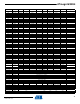
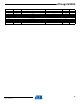
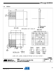
0x1B (0x3B) PCIFR - - - - - - -PCIF0
0x1A (0x3A) Reserved - - - - - - - -
0x19 (0x39) TIFR4 OCF4D OCF4A OCF4B - -TOV4 - -
0x18 (0x38) TIFR3 - - ICF3 - OCF3C OCF3B OCF3A TOV3
0x17 (0x37) Reserved - - - - - - - -
0x16 (0x36) TIFR1
- - ICF1 - OCF1C OCF1B OCF1A TOV1
0x15 (0x35) TIFR0
- - - - - OCF0B OCF0A TOV0
0x14 (0x34) Reserved - - - - - - - -
0x13 (0x33) Reserved - - - - - - - -
0x12 (0x32) Reserved - - - - - - - -
0x11 (0x31) PORTF PORTF7 PORTF6 PORTF5 PORTF4 - - PORTF1 PORTF0
0x10 (0x30) DDRF DDF7 DDF6 DDF5 DDF4 - - DDF1 DDF0
0x0F (0x2F) PINF PINF7 PINF6 PINF5 PINF4 - - PINF1 PINF0
0x0E (0x2E) PORTE - PORTE6 - - - PORTE2 - -
0x0D (0x2D) DDRE - DDE6 - - - DDE2 - -
0x0C (0x2C) PINE - PINE6 - - - PINE2 - -
0x0B (0x2B) PORTD PORTD7 PORTD6 PORTD5 PORTD4 PORTD3 PORTD2 PORTD1 PORTD0
0x0A (0x2A) DDRD
DDD7 DDD6 DDD5 DDD4 DDD3 DDD2 DDD1 DDD0
0x09 (0x29) PIND
PIND7 PIND6 PIND5 PIND4 PIND3 PIND2 PIND1 PIND0
0x08 (0x28) PORTC PORTC7 PORTC6 - - - - - -
0x07 (0x27) DDRC DDC7 DDC6 - - - - - -
0x06 (0x26) PINC PINC7 PINC6 - - - - - -
0x05 (0x25) PORTB PORTB7 PORTB6 PORTB5 PORTB4 PORTB3 PORTB2 PORTB1 PORTB0
0x04 (0x24) DDRB DDB7 DDB6 DDB5 DDB4 DDB3 DDB2 DDB1 DDB0
0x03 (0x23) PINB PINB7 PINB6 PINB5 PINB4 PINB3 PINB2 PINB1 PINB0
0x02 (0x22) Reserved - - - - - - - -
0x01 (0x21) Reserved - - - - - - - -
0x00 (0x20) Reserved - - - - - - - -
Address Name Bit 7 Bit 6 Bit 5 Bit 4 Bit 3 Bit 2 Bit 1 Bit 0 Page