
User Manual

ArduCAM Camera Shield Software Application Note
www.ArduCAM.com
18
7 Registers Table
Sensor and FIFO timing is controlled with a set of registers which is implemented in the
ArduChip. User can send capture commands and read image data with a simple SPI slave interface.
The detail description of registers’ bits can be found in the software section in this document. Not
all the registers are implemented in a given hardware platform, please check the hardware develop
guide for detail register description for certain hardware you've got.
As mentioned earlier the first bit[7] of the command phase is read/write byte, ‘0’ is for read
and ‘1’ is for write, and the bit[6:0] is the address to be read or write in the data phase. So user has
to combine the 8 bits address according to the read or write commands they want to issue.
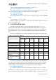
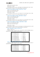
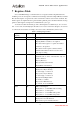
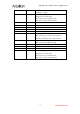
Table 1 ArduChip Register Table
Register Address
bit[6:0]
Register Type
Description
0x00
RW
Test Register
0x01
RW
Capture Control Register
Bit[2:0]: Number of frames to be captured
The value in this register + 1 equal to the number
of frames to be captured.
The value=7 means capture continuous frames
until the frame buffer is full, it is used for short
video clip recording.
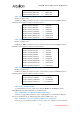
0x02
RW
Bus Mode
Determine who is owner of the data bus, only one
owner is allowed.
Bit[7:2]: Reserved
Bit[1]: Camera write LCD bus
Bit[0]: MCU write LCD bus
0x03
RW
Sensor Interface Timing Register
Bit[0]: Sensor Hsync Polarity,
0 = active high, 1 = active low
Bit[1]: Sensor Vsync Polarity
0 = active high, 1 = active low
Bit[2]: LCD backlight enable
0 = enable, 1 = disable
Bit[3]: Sensor PCLK reverse
0 = normal, 1= reversed PCLK
0x04
RW
FIFO control Register
Bit[0]: write ‘1’ to clear FIFO write done flag
Bit[1]: write ‘1’ to start capture
Bit[4]: write ‘1’ to reset FIFO write pointer
Bit[5]: write ‘1’ to reset FIFO read pointer
0x05
RW
GPIO Direction Register
Bit[0]: Sensor reset IO direction
Bit[1]: Sensor power down IO direction