
Application Notes
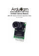

ArduCAM-Mini-5MP-Plus Hardware Application Note
www.ArduCAM.com
6
to combine the 8 bits address according to the read or write commands they want to issue.
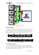
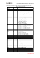
Table 2 ArduChip Register Table
Register Address
bit[6:0]
Register Type
Description
0x00
RW
Test Register
0x01
RW
Capture Control Register
Bit[2:0]: Number of frames to be captured, the
value 0~6 means taking 1~7 photos, the value 7
means continuous capture until the 8MByte frame
buffer is full
0x02
RW
Reserved
0x03
RW
Sensor Interface Timing Register
Bit[0]: Sensor Hsync Polarity,
0 = active high, 1 = active low
Bit[1]: Sensor Vsync Polarity
0 = active high, 1 = active low
Bit[3]: Sensor PCLK reverse
0 = normal, 1= reversed PCLK
0x04
RW
FIFO control Register
Bit[0]: write ‘1’ to clear FIFO write done flag
Bit[1]: write ‘1’ to start capture
Bit[4]: write ‘1’ to reset FIFO write pointer
Bit[5]: write ‘1’ to reset FIFO read pointer
0x05
RW
Reserved
0x06
RW
GPIO Write Register
Bit[0]: Sensor reset IO value
Bit[1]: Sensor power down IO value
Bit[1]: Sensor power enable IO value
0x3B
RO
Reserved
0x3C
RO
Burst FIFO read operation
0x3D
RO
Single FIFO read operation
0x3E
RO
Reserved
0x3F
RO
Reserved
0x40
RO
ArduChip firmware version, constant value 0x62
for 5MP-Plus model
Bit[7:4]: integer part of the revision number
Bit[3:0]: decimal part of the revision number
0x41
RO
Bit[0]: camera vsync pin realtime status
Bit[3]: camera capture done flag
0x42
RO
Camera write FIFO size[7:0]
0x43
RO
Camera write FIFO size[15:8]
0x44
RO
Camera write FIFO size[22:16]
0x45
RO
Reserved