
Application Notes
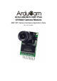

ArduCAM-Mini-5MP-Plus Hardware Application Note
www.ArduCAM.com
5
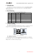
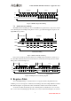
Bit[7] Bit[6] Bit[5] Bit[4] Bit[3] Bit[2] Bit[1] Bit[0] Bit[7] Bit[6] Bit[5] Bit[4] Bit[3] Bit[2] Bit[1] Bit[0]
SCLK
MOSI
CSn
MISO
Command Phase Data Phase
Bus Read Timing
Bit[7] Bit[6] Bit[5] Bit[4] Bit[3] Bit[2] Bit[1] Bit[0]
Figure 8 SPI Bus Single Read Timing
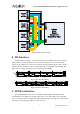
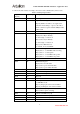
7.3 SPI Bus Burst Read Timing
The SPI bus burst read timing is only for burst FIFO read operation. It is composed of a burst
read command phase and multiple data phases in order to get double throughput compared to the
single FIFO read operation.
CMD 0x00 0x00 0x00 0x00 0x00 0x00 0x00
SCLK
MOSI
CSn
MISO
Command Phase
Data Phase
Bus Burst Read Timing
D1 D2 D3 Dn-2 Dn-1 Dn
D0
Figure 9 SPI Bus Burst Read Timing
If user want to break up the burst transaction by multiple burst read. Please note that do not
use other SPI command between burst read transactions, it will cause the image data lost. Detail
timing can be found from Figure 10.
CMD 0x00 0x00 0x00 0x00 0x00 0x00 0x00
SCLK
MOSI
CSn
MISO
Command Phase
Data Phase
D0 D1 D2
Dn-2 Dn-1 Dn
CMD 0x00 0x00 0x00 0x00 0x00 0x00 0x00
Command Phase
Data Phase
Dn+1
Dn+2 Dn+3 Dn+4 Dm-2 Dm-1 Dm
First read transaction
following read transaction
D3
Figure 10 Multiple burst read timing diagram
8 Registers Table
Sensor and FIFO timing is controlled with a set of registers which is implemented in the
ArduChip. User can send capture commands and read image data with a simple SPI slave interface.
The detail description of registers’ bits can be found in the software section in this document.
As mentioned earlier the first bit[7] of the command phase is read/write byte, ‘0’ is for read
and ‘1’ is for write, and the bit[6:0] is the address to be read or write in the data phase. So user has