
Application Notes

ArduCAM-Mini-5MP-Plus Hardware Application Note
www.ArduCAM.com
4
The first bit[7] of the command phase is read/write byte, ‘0’ is for read and ‘1’ is for write,
and the bit[6:0] is the address to be read or write in the data phase. ArduChip register table see
Table 1.
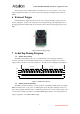
6 External Trigger
External hardware trigger input can be used to start a capture manually, software part only
needs to polling the "capture done" status bit before reading the image data. The Figure 6 shows
the trigger pin which is marked with "T" at the back of the module, and the trigger input is active
high.
Figure 6 External Trigger Input
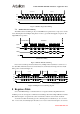
7 ArduChip Timing Diagram
7.1 SPI Bus Write Timing
The SPI bus write timing composed of a command phase and a data phase during the
assertion of the chip select signal CSn. The first 8 bits is command byte which is decoded as a
register address, and the second 8 bits is data byte to be written to the ArduChip internal registers.
Bit[7] Bit[6] Bit[5] Bit[4] Bit[3] Bit[2] Bit[1] Bit[0] Bit[7] Bit[6] Bit[5] Bit[4] Bit[3] Bit[2] Bit[1] Bit[0]
SCLK
MOSI
CSn
MISO
Command Phase Data Phase
Bus Write Timing
Don’t Care
Figure 7 SPI Bus Write Timing
7.2 SPI Bus Single Read Timing
The SPI bus single read timing is for read operation of ArduChip internal registers and single
FIFO read function. It is composed of a command phase and a data phase during the assertion of
chip select signal CSn. The first 8 bits is command byte which is decoded as a register address, the
second 8 bits is dummy byte written to the SPI bus MOSI signal, and the content read back from
register is appeared on the SPI bus MISO signal.