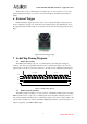
ArduCAM-Mini-5MP-Plus OV5642 Camera Module 5MP SPI Camera Hardware Application Note Rev 1.
ArduCAM-Mini-5MP-Plus Hardware Application Note Table of Contents 1 2 3 3.1 3.2 4 5 6 7 7.1 7.2 7.3 8 Introduction ............................................................................................................................. 2 Pin Definition ........................................................................................................................... 2 Typical Wiring ...............................................................................................................
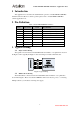
ArduCAM-Mini-5MP-Plus Hardware Application Note 1 Introduction This application note describes the detail hardware operation of ArduCAM-Mini-5MP-Plus OV5642 camera module. For software operation please refer to ArduCAM-Mini-5MP-Plus software application note. 2 Pin Definition Table 1 ArduCAM-M-5MP Pin Definition Pin No.
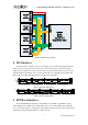
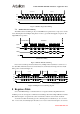
ArduCAM-Mini-5MP-Plus Hardware Application Note VCC GND ArduCAM SCL SDA Mini CSn 5MP-Plus MISO MOSI SCLK VCC GND +5V GND SCL SDA MISO MOSI SCLK ArduCAM SCL SDA Mini CSn 5MP-Plus MISO MOSI SCLK VCC GND ArduCAM SCL SDA Mini CSn 5MP-Plus MISO MOSI SCLK Arduino Maple Chipkit Raspberry Pi BeagleBone Black CS0n CS1n CS2n CS3n VCC GND ArduCAM SCL SDA Mini CSn 5MP-Plus MISO MOSI SCLK Figure 3 Multi-Cameras Wiring 4 I2C Interface The I2C interface is directly connected to the image sensor OV5642.
ArduCAM-Mini-5MP-Plus Hardware Application Note The first bit[7] of the command phase is read/write byte, ‘0’ is for read and ‘1’ is for write, and the bit[6:0] is the address to be read or write in the data phase. ArduChip register table see Table 1. 6 External Trigger External hardware trigger input can be used to start a capture manually, software part only needs to polling the "capture done" status bit before reading the image data.
ArduCAM-Mini-5MP-Plus Hardware Application Note Command Phase Data Phase SCLK MOSI Bit[7] Bit[6] Bit[5] Bit[4] Bit[3] Bit[2] Bit[1] Bit[0] MISO Bit[7] Bit[6] Bit[5] Bit[4] Bit[3] Bit[2] Bit[1] Bit[0] Bit[7] Bit[6] Bit[5] Bit[4] Bit[3] Bit[2] Bit[1] Bit[0] CSn Bus Read Timing Figure 8 SPI Bus Single Read Timing 7.3 SPI Bus Burst Read Timing The SPI bus burst read timing is only for burst FIFO read operation.
ArduCAM-Mini-5MP-Plus Hardware Application Note to combine the 8 bits address according to the read or write commands they want to issue.
ArduCAM-Mini-5MP-Plus Hardware Application Note 7 www.ArduCAM.