
Application Notes

ArduCAM-M-2MP Hardware Application Note
www.ArduCAM.com
5
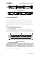
Figure 8 SPI Bus Single Read Timing
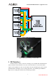
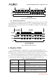
5.3 SPI Bus Burst Read Timing
The SPI bus burst read timing is only for burst FIFO read operation. It is composed of a burst
read command phase and multiple data phases in order to get double throughput compared to the
single FIFO read operation. The first byte read from the FIFO is a dummy byte, and the following
bytes are valid bytes.
Figure 9 SPI Bus Burst Read Timing
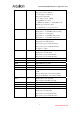
6 Registers Table
Sensor and FIFO timing is controlled with a set of registers which is implemented in the
ArduChip. User can send capture commands and read image data with a simple SPI slave interface.
The detail description of registers’ bits can be found in the software section in this document.
As mentioned earlier the first bit[7] of the command phase is read/write byte, ‘0’ is for read
and ‘1’ is for write, and the bit[6:0] is the address to be read or write in the data phase. So user has
to combine the 8 bits address according to the read or write commands they want to issue.
Table 1 ArduChip Register Table
Register Address
bit[6:0]
Register Type Description
0x00 RW Test Register
0x01 RW Capture Control Register
Bit[2:0]: Number of frames to be captured
0x02 RW Reserved
0x03 RW Sensor Interface Timing Register
Bit[0]: Sensor Hsync Polarity,