
Application Notes

ArduCAM-M-2MP Hardware Application Note
www.ArduCAM.com
4
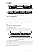
Figure 5 I2C Write Bus Timing
Figure 6 I2C Read Bus Timing
4 SPI Slave Interface
The ArduCAM SPI slave interface is fixed SPI mode 0 with POL = 0 and PHA = 1. The
maximum speed of SCLK is designed for 8MHz, care should taken do not over clock the
maximum 8MHz. The SPI protocol is designed with a command phase with variable data phase.
The chip select signal should always keep asserted during the SPI read or write bus cycle.
The first bit[7] of the command phase is read/write byte, ‘0’ is for read and ‘1’ is for write,
and the bit[6:0] is the address to be read or write in the data phase. ArduChip register table see
Table 1.
5 ArduChip Timing Diagram
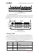
5.1 SPI Bus Write Timing
The SPI bus write timing composed of a command phase and a data phase during the
assertion of the chip select signal CSn. The first 8 bits is command byte which is decoded as a
register address, and the second 8 bits is data byte to be written to the ArduChip internal registers.
Figure 7 SPI Bus Write Timing
5.2 SPI Bus Single Read Timing
The SPI bus single read timing is for read operation of ArduChip internal registers and single
FIFO read function. It is composed of a command phase and a data phase during the assertion of
chip select signal CSn. The first 8 bits is command byte which is decoded as a register address, the
second 8 bits is dummy byte written to the SPI bus MOSI signal, and the content read back from
register is appeared on the SPI bus MISO signal.