
Low Distortion IMX219 M12 Mount Camera Module for Raspberry Pi - Datasheet
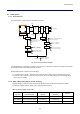
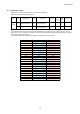
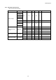
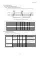
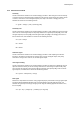
Table Of Contents
- Description
- Features
- Device Structure
- USE RESTRICTION NOTICE
- 1. Block Diagram and Pin Configuration
- 2. Pixel Signal Output Specifications
- 3. Control Registers
- 3-1 2-wire Serial Communication Operation Specifications
- 3-2 2-wire Serial Communication Register Map (Configuration register, Parameter limit register)
- 3-3 Parameter Limit Registers – [0x1000-0x1FFF] (Read Only and Static)
- 3-4 Manufacturer Specific Registers – [0x3000-0x5FFF ]
- 3-5 Frame Bank A and Bank B specific output samples
- 4. Output Data Format
- 6. On Chip Image Processing
- 7. NVM Memory Map
- 8. How to operate IMX219PQH5-C
- 9. Other Functions
- 10. Electrical Characteristics
- 11. Spectral Sensitivity Characteristic
- 12. Image Sensor Characteristics
- 13. Measurement Method for Image Sensor Characteristics
- 14. Spot Pixel Specification
- 15. Notice on White Pixels Specifications
- 16. Chief Ray Angle Characteristics
- 17. Connection Example
- 18. Notes On Handling

IMX219PQH5-C
81
9. Other Functions
9-1 Clock System
9-1-1 Clock Structure
The IMX219PQH5-C clock system has the following structure.
ADC
Pipe
Line
FiFo Mipi
Control Unit
INCK
Data Out
2Ch
10
SYSCLK
OUT_CLK
mipi_CL
K
PIX_CL
K
10
10
10
0x030CPLL_OP_MPY[10:8]
0x030D:PLL_OP_MPY[7:0]
0x0304=1(1/1), 2(1/2) or 3(1/3)
automatically for EXCK_FREQ
0x0306:PLL_VT_MPY[10:8]
0x0307:PLL_VT_MPY[7:0]
0x0301:VTPXCK_DIV
=4(1/4), 5(1/5), 8(1/8) or 10(1/10)
0x0303:VTSYCK_DIV
=1(1/1)
0x0309:OPPXCK_DIV=8(1/8) or 10(1/10)
0x030B:OPSYCK_DIV=1(1/2)
DIV2
PLL2
Pre-Div2
Pre-Div1
PLL1
DIV1
0x012A:EXCK_FREQ[15:8]
0x012B:EXCK_FREQ[7:0]
0x0305=1(1/1), 2(1/2) or 3(1/3)
automatically for EXCK_FREQ
Fig. 43 Clock System Block Diagram
The IMX219PQH5-C is comprised of 2 ch Pipe-Line, and 2 PLL for both pixel read domain and Output data domain.
See following section (Clock Setting Example) for detail.
Relationships between 2 domains are the followings;
1 If, Pix Rate of PLL1 domain < Data Rate of PLL2 domain, data is always correctly output from the sensor
2 If Pix Rate of PLL1 domain > Data rate of PLL2 domain, Else If de-rating (binning and sub-sampling without
resize), FiFo can handle.
9-1-2 EXCK_FREQ setting depend on INCK frequency
The IMX219PQH5-C has the function that automatically set Pre-Div1 and Pre-Div2 by setting the register
by setting the register of EXCK_FREQ, case of changing INCK frequency.
Table 39 EXCK_FREQ setting table
INCK
(Input Pin)
EXCK_FREQ
(0x012A/0x012B)
PREPLLCK_VT_DIV
(0x0304)
PREPLLCK_OP_DIV
(0x0305)
Remark
6 to 12[MHz]
6d to 12d (06h to 0Ch)
01h (auto set)
01h (auto set)
12 to 24[MHz]
12d to 24d (0Ch to 18h)
02h (auto set)
02h (auto set)
24 to 27[MHz]
24d to 27d (18h to 1Bh)
03h (auto set)
03h (auto set)