
Low Distortion IMX219 M12 Mount Camera Module for Raspberry Pi - Datasheet
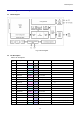
Table Of Contents
- Description
- Features
- Device Structure
- USE RESTRICTION NOTICE
- 1. Block Diagram and Pin Configuration
- 2. Pixel Signal Output Specifications
- 3. Control Registers
- 3-1 2-wire Serial Communication Operation Specifications
- 3-2 2-wire Serial Communication Register Map (Configuration register, Parameter limit register)
- 3-3 Parameter Limit Registers – [0x1000-0x1FFF] (Read Only and Static)
- 3-4 Manufacturer Specific Registers – [0x3000-0x5FFF ]
- 3-5 Frame Bank A and Bank B specific output samples
- 4. Output Data Format
- 6. On Chip Image Processing
- 7. NVM Memory Map
- 8. How to operate IMX219PQH5-C
- 9. Other Functions
- 10. Electrical Characteristics
- 11. Spectral Sensitivity Characteristic
- 12. Image Sensor Characteristics
- 13. Measurement Method for Image Sensor Characteristics
- 14. Spot Pixel Specification
- 15. Notice on White Pixels Specifications
- 16. Chief Ray Angle Characteristics
- 17. Connection Example
- 18. Notes On Handling
IMX219PQH5-C
8
Fig. 39 Start streaming sequence with 2-wire serial communication (external reset) ................................ 78
Fig. 40 Power-off Sequence in 2-wire Serial Communication ................................................................... 79
Fig. 41 Software Standby Operation Pattern 1 ........................................................................................ 80
Fig. 42 Software Standby Operation Pattern 2 ........................................................................................ 80
Fig. 43 Clock System Block Diagram ...................................................................................................... 81
Fig. 44 Master Clock Square Waveform Diagram .................................................................................... 86
Fig. 45 Spectral sensitivity characteristics ............................................................................................... 87
Fig. 46 Zone Definition Diagram .............................................................................................................. 88
Fig. 47 Color coding alignment................................................................................................................ 89
Fig. 48 Measurement Method for Spot Pixels .......................................................................................... 93
Fig. 49 Chief Ray Angle Characteristics .................................................................................................. 94
Fig. 50 Recommended Circuit ................................................................................................................. 95
Tables
Table 1 Pin Description ........................................................................................................................... 10
Table 2 Pin Coordinates .......................................................................................................................... 15
Table 3 Description of 2-wire Serial Communication Pins ........................................................................ 17
Table 4 R/W Bit ....................................................................................................................................... 18
Table 5 2-wire Serial Communication Address Space.............................................................................. 19
Table 6 Operations Supported by 2-wire Serial Communication .............................................................. 19
Table 7 2-wire Serial Communication Operation Specifications ............................................................... 23
Table 8 2-wire Serial Communication AC Timing (Fast mode plus (INCK[fSCK] = 11.4 to 27 MHz)) ......... 23
Table 9 2-wire Serial Communication AC Timing (Fast mode) .................................................................. 24
Table 10 2-wire Serial Communication Register Map Address Areas ....................................................... 24
Table 11 Access command sequence...................................................................................................... 41
Table 12 Number of CSI lane Setting Registers ....................................................................................... 47
Table 13 Image pixel area and data type ................................................................................................. 49
Table 14 Sync Code Settings .................................................................................................................. 49
Table 15 Embedded Data Line Tag ......................................................................................................... 51
Table 16 Mode example .......................................................................................................................... 53
Table 17 Image Orientation Register ....................................................................................................... 55
Table 18 Gain Setting Variables .............................................................................................................. 56
Table 19 Storage Time Setting Register .................................................................................................. 56
Table 20 Storage Time Offset Register.................................................................................................... 56
Table 21 Storage Time Setting (in case of Line_Length_pck = 3448) ....................................................... 57
Table 22 Gain Setting Variables .............................................................................................................. 58
Table 23 Analogue Gain Setting .............................................................................................................. 59
Table 24 Digital Gain Settings ................................................................................................................. 60
Table 25 Example of Digital Gain Setting ................................................................................................ 61