
Low Distortion IMX219 M12 Mount Camera Module for Raspberry Pi - Datasheet
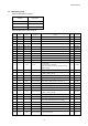
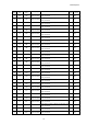
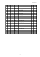
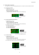
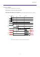
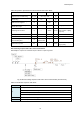
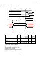
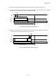
Table Of Contents
- Description
- Features
- Device Structure
- USE RESTRICTION NOTICE
- 1. Block Diagram and Pin Configuration
- 2. Pixel Signal Output Specifications
- 3. Control Registers
- 3-1 2-wire Serial Communication Operation Specifications
- 3-2 2-wire Serial Communication Register Map (Configuration register, Parameter limit register)
- 3-3 Parameter Limit Registers – [0x1000-0x1FFF] (Read Only and Static)
- 3-4 Manufacturer Specific Registers – [0x3000-0x5FFF ]
- 3-5 Frame Bank A and Bank B specific output samples
- 4. Output Data Format
- 6. On Chip Image Processing
- 7. NVM Memory Map
- 8. How to operate IMX219PQH5-C
- 9. Other Functions
- 10. Electrical Characteristics
- 11. Spectral Sensitivity Characteristic
- 12. Image Sensor Characteristics
- 13. Measurement Method for Image Sensor Characteristics
- 14. Spot Pixel Specification
- 15. Notice on White Pixels Specifications
- 16. Chief Ray Angle Characteristics
- 17. Connection Example
- 18. Notes On Handling

IMX219PQH5-C
75
7-5 Defects Address registration
The single defect, the same color adjoining (SCA) defect and 2 x 4 defect are stored into NVM and corrected.
7-5-1 Single defect address
1. Target Address; (x, y) = (xt, yt)
*Output area is Effective Area
Output size is 3280x2464 (0,0) - (3279,2463)
x = image area address + offset; offset = 8d
y = image area address + offset; offset = 48d (not include embedded lines)
Fig. 35 Single defect
7-5-2 Same Color Adjoining defect address
1. Target Address; (x, y) = (xt, yt)
*Output area is Effective Area
Output size is 3280x2464 (0,0) - (3279,2463)
x = image area address + offset; offset = 8d
y = image area address + offset; offset = 48d (not include embedded lines)
2. Directions are also described in the following figure
0d = defect in right adjoining
1d = defect in right bottom adjoining
2d = defect in bottom adjoining
3d = defect in left bottom adjoining
Fig. 36 Same Color Adjoining defect
7-5-3 2x4 defect address
1. Target Address; (x, y) = (xt, yt)
*Output area is Effective Area
Output size is 3280x2464 (0,0) - (3279,2463)
x = image area address + offset; offset = 8d
y = image area address + offset; offset = 48d (not include embedded lines)
2. Only upper left pixel address needed in this case, always RED pixels
Fig. 37 2x4 defect
x
Scan Direction
Image Orientation = 0d
Starting Red Pixel Data
x
Scan Direction
Image Orientation = 0d
Starting Red Pixel Data
0
3 2 1
x
Scan Direction
Image Orientation = 0d
Starting Red Pixel Data