
Low Distortion IMX219 M12 Mount Camera Module for Raspberry Pi - Datasheet
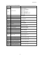


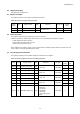
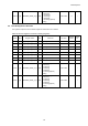
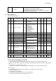
Table Of Contents
- Description
- Features
- Device Structure
- USE RESTRICTION NOTICE
- 1. Block Diagram and Pin Configuration
- 2. Pixel Signal Output Specifications
- 3. Control Registers
- 3-1 2-wire Serial Communication Operation Specifications
- 3-2 2-wire Serial Communication Register Map (Configuration register, Parameter limit register)
- 3-3 Parameter Limit Registers – [0x1000-0x1FFF] (Read Only and Static)
- 3-4 Manufacturer Specific Registers – [0x3000-0x5FFF ]
- 3-5 Frame Bank A and Bank B specific output samples
- 4. Output Data Format
- 6. On Chip Image Processing
- 7. NVM Memory Map
- 8. How to operate IMX219PQH5-C
- 9. Other Functions
- 10. Electrical Characteristics
- 11. Spectral Sensitivity Characteristic
- 12. Image Sensor Characteristics
- 13. Measurement Method for Image Sensor Characteristics
- 14. Spot Pixel Specification
- 15. Notice on White Pixels Specifications
- 16. Chief Ray Angle Characteristics
- 17. Connection Example
- 18. Notes On Handling

IMX219PQH5-C
70
6
ECC status
Can check while reading/writing that ECC is applied by page.
1. Read data is correct. No ECC is applied.
2. Read data is correct with 1-bit correction of ECC.
3. Read data is incorrect though ECC is applied (means >2 bits per a
unit of 16-byte (row) are incorrect).
7-3 Related Registers
Table 32 Related Registers
Index
Byte
Register Name
RW
Comment
Re-Time
Default
(HEX)
Embd
DL
Comments
0100
[0]
Mode_sel
RW
Mode select
0: SW- Standby
1: Streaming
0
3300
[7:0]
SYSOTP_IF_MODE1
RW
OTP mode setting
[1:0]: control access cycle to
fuse cell
00: INCK cycle
01: INCK/2 cycle
10: INCK/4 cycle
11: INCK/8 cycle
[3]: ECC disable switch
0: ECC on,1:ECC off
[5]:write mode;
0: test mode
1: recommended
00
5E54
[7:0]
OUTF
RW
Monitor Output Enable
C0
5E59
[7:0]
TESTMNT1
RW
Monitor Output
00
4053
[7:0]
TEST_FSTRB
RW
Set FStrobe pin to monitor
00
012A
[7:0]
EXCK_FREQ [15:8]
RW
input_clk_frequency_mhz
(default = 7.6[MHz])
07
012B
[7:0]
EXCK_FREQ [7:0]
RW
99
3302
[7:0]
SYSOTP_IF_WRCNT[15:8]
RW
OTP write clock setting
00
3303
[7:0]
SYSOTP_IF_WRCNT[7:0]
RW
00
3200
[2:0]
OTPIF_CTRL
RW
OTP I/F control register
[0] enable [1]R/W [2]error
clear
0
3201
[1:0]
OTPIF_STATUS
RO-D
OTP I/F status; [0] read ready
[1] write ready
[2] 0: normal
1: Data error exists, and
cannot be corrected by ECC.
Read data is incorrect.
0
3202
[2:0]
OTPIF_PAGE_SELECT
RW
otpif_page_select
0
3204
[7:0]
OTPIF_DT_0
RW
otpif_data_0
00
(DT_1 to DT_62)
3243
[7:0]
OTPIF_DT_63
RW
otpif_data_63
00
Trigger to
start write
sequence
Before writing / reading following steps are required
1. Set Sensor being SW-Standby by 0x0100 = 0h
2. Wait one frame time (See t0 in 8-2 Power off sequence session) when previous status is streaming.
3. Set monitor output to check writing pulse by 0x5E54=00h and 0x5E59=FFh, 4053=0Ah. (option, debug purpose
only)
4. Set OTP write clock setting. (target = 25 µS)
(When INCK = 12.0 MHz, wrcnt should be set to 012Ch (target = 25µs : 300d) at 0x3302, 0x3303)
Then when writing;
1. Set controller "ECC ON" or ECC OFF" by 0x3300 = "20h" (ECC ON) or "28h" (ECC OFF)
2. Set Write by 0x3200 = "3h."
3. Set page from 0 to 11 by 0x3202.
4. Set 0x3204 to 0x3243 OTPIF_DT_0to 63 = xxh (Data to Write)
Please overwrite all values when you program next page.