
Low Distortion IMX219 M12 Mount Camera Module for Raspberry Pi - Datasheet
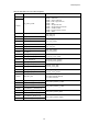
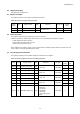
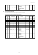
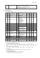
Table Of Contents
- Description
- Features
- Device Structure
- USE RESTRICTION NOTICE
- 1. Block Diagram and Pin Configuration
- 2. Pixel Signal Output Specifications
- 3. Control Registers
- 3-1 2-wire Serial Communication Operation Specifications
- 3-2 2-wire Serial Communication Register Map (Configuration register, Parameter limit register)
- 3-3 Parameter Limit Registers – [0x1000-0x1FFF] (Read Only and Static)
- 3-4 Manufacturer Specific Registers – [0x3000-0x5FFF ]
- 3-5 Frame Bank A and Bank B specific output samples
- 4. Output Data Format
- 6. On Chip Image Processing
- 7. NVM Memory Map
- 8. How to operate IMX219PQH5-C
- 9. Other Functions
- 10. Electrical Characteristics
- 11. Spectral Sensitivity Characteristic
- 12. Image Sensor Characteristics
- 13. Measurement Method for Image Sensor Characteristics
- 14. Spot Pixel Specification
- 15. Notice on White Pixels Specifications
- 16. Chief Ray Angle Characteristics
- 17. Connection Example
- 18. Notes On Handling

IMX219PQH5-C
67
6-2 Digital Gain Setting
See Digital gain settings section.
6-3 Black Level Adjust
The register required to set the Black Level Adjust is as follows.
Table 28 Black Level Adjust Setting Register
Index
(HEX)
Bit
Register Name
RW
Comment
Re-Timed
Default
(HEX)
D1EA
[1:0]
DT_PEDESTAL[9:8]
RW
Set Black Level
0
D1EB
[7:0]
DT_PEDESTAL[7:0]
RW
40
6-4 Defect Correction
The registers required to set the Defect Correction are as follows.
3 different functions are implemented; (Please refer to 7-5 Defects Address registration session);
1.Static single defect pixel correction
2.Static same color adjoin pixel correction
3.Static 2x4 defect pixel correction
Defect addresses for mapped_couplet_correct (couplet defect: two adjacent defect pixels of the same color) are
stored in NVM , and sensor processes them in itself.
6-5 Pixel Re-alignment H Direction
The registers required to set the Pixel Re-alignment H Direction are as follows.
Table 29 Pixel Re-alignment H Direction Setting Registers
Index
Byte
Register Name
RW
Comment
Re-Time
Default
(HEX)
Embd
DL
0x0164
[3:0]
X_ADD_STA_A[11:8]
RW
x_addr_start
Frame Bank
0
0x0165
[7:0]
X_ADD_STA_A[7:0]
RW
00
0x0166
[3:0]
X_ADD_END_A[11:8]
RW
x_addr_end
Frame Bank
C
0x0167
[7:0]
X_ADD_END_A[7:0]
RW
CF
0x0264
[3:0]
X_ADD_STA_B[11:8]
RW
x_addr_start
Frame Bank
0
0x0265
[7:0]
X_ADD_STA_B[7:0]
RW
00
0x0266
[3:0]
X_ADD_END_B[11:8]
RW
x_addr_end
Frame Bank
C
0x0267
[7:0]
X_ADD_END_B[7:0]
RW
CF
0x0174
[0]
BINNING_MODE_H_A
RW
defines binning mode
(H-direction).
0: no-binning,
1: x2-binning
2: x4-binning
3: x2-analog (special)
binning
Frame Bank
0