
Low Distortion IMX219 M12 Mount Camera Module for Raspberry Pi - Datasheet
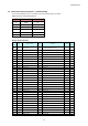
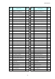
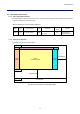
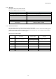
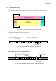
Table Of Contents
- Description
- Features
- Device Structure
- USE RESTRICTION NOTICE
- 1. Block Diagram and Pin Configuration
- 2. Pixel Signal Output Specifications
- 3. Control Registers
- 3-1 2-wire Serial Communication Operation Specifications
- 3-2 2-wire Serial Communication Register Map (Configuration register, Parameter limit register)
- 3-3 Parameter Limit Registers – [0x1000-0x1FFF] (Read Only and Static)
- 3-4 Manufacturer Specific Registers – [0x3000-0x5FFF ]
- 3-5 Frame Bank A and Bank B specific output samples
- 4. Output Data Format
- 6. On Chip Image Processing
- 7. NVM Memory Map
- 8. How to operate IMX219PQH5-C
- 9. Other Functions
- 10. Electrical Characteristics
- 11. Spectral Sensitivity Characteristic
- 12. Image Sensor Characteristics
- 13. Measurement Method for Image Sensor Characteristics
- 14. Spot Pixel Specification
- 15. Notice on White Pixels Specifications
- 16. Chief Ray Angle Characteristics
- 17. Connection Example
- 18. Notes On Handling

IMX219PQH5-C
47
4. Output Data Format
4-1 CSI-2 Output Data Format
4-1-1 CSI-2 Output Data Channels
The IMX219PQH5-C can select the CSI-2 2 lanes or CSI-2 4 lanes serial signal output method that uses all pairs
of differential signals for image data output.
Table 12 Number of CSI lane Setting Registers
Index
Byte
Register Name
RW
Comment
Default
(HEX)
Remark
0x0114
[1:0]
CSI_LANE_MODE
RW
03: 4Lane
01: 2Lane
03
Setting before
standby cancel
4-1-2 CSI-2 Frame Structure
The image frame structure is shown below.
Fig. 20 Frame Structure for Serial signal output
FS
FE
Pixels
(effective pixels)
line blanking
frame blanking
Next Frame
FS
Packet
Header
Packet
Footer
Embedded Data LinesPH
PF