
Low Distortion IMX219 M12 Mount Camera Module for Raspberry Pi - Datasheet
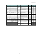
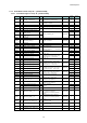
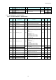
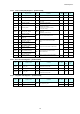
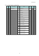
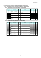
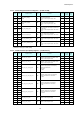
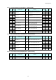
Table Of Contents
- Description
- Features
- Device Structure
- USE RESTRICTION NOTICE
- 1. Block Diagram and Pin Configuration
- 2. Pixel Signal Output Specifications
- 3. Control Registers
- 3-1 2-wire Serial Communication Operation Specifications
- 3-2 2-wire Serial Communication Register Map (Configuration register, Parameter limit register)
- 3-3 Parameter Limit Registers – [0x1000-0x1FFF] (Read Only and Static)
- 3-4 Manufacturer Specific Registers – [0x3000-0x5FFF ]
- 3-5 Frame Bank A and Bank B specific output samples
- 4. Output Data Format
- 6. On Chip Image Processing
- 7. NVM Memory Map
- 8. How to operate IMX219PQH5-C
- 9. Other Functions
- 10. Electrical Characteristics
- 11. Spectral Sensitivity Characteristic
- 12. Image Sensor Characteristics
- 13. Measurement Method for Image Sensor Characteristics
- 14. Spot Pixel Specification
- 15. Notice on White Pixels Specifications
- 16. Chief Ray Angle Characteristics
- 17. Connection Example
- 18. Notes On Handling

IMX219PQH5-C
39
3-3-1-5 Frame Timing Parameter Limit Registers – [0x1140-0x114B]
Index
Byte
Register Name
RW
Comment
Re-Time
Default
(HEX)
Embd
DL
0x1140
[7:0]
min_frame_length_
lines
RO
Minimum Frame Length allowed. Value
both sensor dependent
Format: 16-bit unsigned integer Units:
Lines
01
0x1141
[7:0]
00
0x1142
[7:0]
max_frame_length_
lines
RO
Maximum possible number of lines per
Frame. Value sensor dependent
Format: 16-bit unsigned integer Units:
Lines
FF
0x1143
[7:0]
FE
0x1144
[7:0]
min_line_length_pck
RO
Minimum Line Length allowed. Value
sensor dependent. But setup is possible at a
smaller value *
Format: 16-bit unsigned integer Units: Pixel
Clock
0D
0x1145
[7:0]
78
0x1146
[7:0]
max_line_length_pck
RO
Maximum possible number of pixel clocks
per line. Value sensor dependent
Format: 16-bit unsigned integer Units: Pixel
Clock
7F
0x1147
[7:0]
F0
0x1148
[7:0]
min_line_blanking_pck
RO
Minimum line blanking time in pixel clocks
Format: 16-bit unsigned integer Units: Pixel
Clock
00
0x1149
[7:0]
A8
0x114A
[7:0]
min_frame_blanking_lines
RO
Minimum frame blanking in video timing
lines
Format: 16-bit unsigned integer Units: Pixel
Clock
00
0x114B
[7:0]
20
* possible to setup up to D60 (HEX)
3-3-1-6 Output Clock Set-up Capability Registers – [0x1160-0x1177]
Index
Byte
Register Name
RW
Comment
Re-Time
Default
(HEX)
Embd
DL
0x1160
[7:0]
min_op_sys_clk_div
RO
Minimum output system clock divider value
Format: 16-bit unsigned integer
00
0x1161
[7:0]
01
0x1162
[7:0]
max_op_sys_clk_div
RO
Maximum output system clock divider value
Format: 16-bit unsigned integer
00
0x1163
[7:0]
02
0x1164
[7:0]
min_op_sys_clk_freq_mhz
RO
Minimum output system clock frequency
Format: IEEE 32-bit float
Units: MHz
200 MHz
43
0x1165
[7:0]
48
0x1166
[7:0]
00
0x1167
[7:0]
00
0x1168
[7:0]
max_op_sys_clk_freq_mhz
RO
Maximum output system clock frequency
Format: IEEE 32-bit float Units: MHz
916 MHz
44
0x1169
[7:0]
65
0x116A
[7:0]
20
0x116B
[7:0]
00
0x116C
[7:0]
min_op_pix_clk_freq_mhz
RO
Minimum output pixel clock frequency
Format: IEEE 32-bit float Units: MHz
20 MHz
41
0x116D
[7:0]
A0
0x116E
[7:0]
00
0x116F
[7:0]
00
0x1170
[7:0]
max_op_pix_clk_freq_mhz
RO
Maximum output pixel clock frequency
Format: IEEE 32-bit float Units: MHz
114.5 MHz
42
0x1171
[7:0]
E5
0x1172
[7:0]
00
0x1173
[7:0]
00
0x1174
[7:0]
min_op_pix_clk_div
RO
Minimum output pixel clock divider value
Format: 16-bit unsigned integer
00
0x1175
[7:0]
08
0x1176
[7:0]
max_op_pix_clk_div
RO
Maximum output pixel clock divider value
Format: 16-bit unsigned integer
00
0x1177
[7:0]
0A