
Low Distortion IMX219 M12 Mount Camera Module for Raspberry Pi - Datasheet
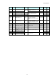
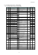
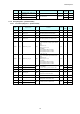
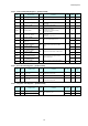
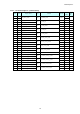
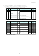
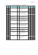
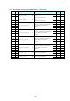
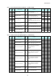
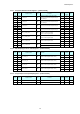
Table Of Contents
- Description
- Features
- Device Structure
- USE RESTRICTION NOTICE
- 1. Block Diagram and Pin Configuration
- 2. Pixel Signal Output Specifications
- 3. Control Registers
- 3-1 2-wire Serial Communication Operation Specifications
- 3-2 2-wire Serial Communication Register Map (Configuration register, Parameter limit register)
- 3-3 Parameter Limit Registers – [0x1000-0x1FFF] (Read Only and Static)
- 3-4 Manufacturer Specific Registers – [0x3000-0x5FFF ]
- 3-5 Frame Bank A and Bank B specific output samples
- 4. Output Data Format
- 6. On Chip Image Processing
- 7. NVM Memory Map
- 8. How to operate IMX219PQH5-C
- 9. Other Functions
- 10. Electrical Characteristics
- 11. Spectral Sensitivity Characteristic
- 12. Image Sensor Characteristics
- 13. Measurement Method for Image Sensor Characteristics
- 14. Spot Pixel Specification
- 15. Notice on White Pixels Specifications
- 16. Chief Ray Angle Characteristics
- 17. Connection Example
- 18. Notes On Handling

IMX219PQH5-C
32
3-2-4 Frame Bank Control Group “B” – [0x0254-0x028D]
3-2-4-1 Frame Bank Registers Group “B”- [0x0254-0x028D]
Index
Byte
Register Name
RW
Comment
Re-Time
Default
(HEX)
Embd
DL
0x0254
[7:0]
FRAME_DURATION_B
RW
defines number of frames to apply
FrameBank-A to actual function.
frame bank
00
0x0255
[0]
COMP_ENABLE_B
RW
compression 10 to 8 mode
0: Disable, 1: Enable
frame bank
0
0x0256
0x0257
[7:0]
ANA_GAIN_GLOBAL_B
RW
analogue_gain_code_global
frame bank
00
0x0258
[3:0]
DIG_GAIN_GLOBAL_B[11:8]
RW
digital gain global
frame bank
1
0x0259
[7:0]
DIG_GAIN_GLOBAL_B[7:0]
00
0x025A
[7:0]
COARSE_INTEGRATION_
TIME_B[15:8]
RW
coarse_integration_time
frame bank
03
0x025B
[7:0]
COARSE_INTEGRATION_
TIME_B[7:0]
RW
E8
0x025C
Reserved
0x025D
[0]
SENSOR_MODE_B
RO
shutter mode register.
0: ERS, 1: reserved
frame bank
0
0x025E
Reserved
0x025F
Reserved
0x0260
[7:0]
FRM_LENGTH_B[15:8]
RW
frame_length_lines
BINNING_MODE = 0,1,2 Unit:1Lines
BINNING_MODE = 3 Units:2Lines
frame bank
0A
0x0261
[7:0]
FRM_LENGTH_B[7:0]
A8
0x0262
[7:0]
LINE_LENGTH_B[15:8]
RW
line_length_pck
Units: Pixels
frame bank
0D
0x0263
[7:0]
LINE_LENGTH_B[7:0]
78
0x0264
[3:0]
X_ADD_STA_B[11:8]
RW
x_addr_start
X-address of the top left corner of the
visible pixel data Units: Pixels
frame bank
0
0x0265
[7:0]
X_ADD_STA_B[7:0]
00
0x0266
[3:0]
X_ADD_END_B[11:8]
RW
x_addr_end
X-address of the bottom right corner of
the visible pixel data Units: Pixels
frame bank
C
0x0267
[7:0]
X_ADD_END_B[7:0]
CF
0x0268
[3:0]
Y_ADD_STA_B[11:8]
RW
y_addr_start
Y-address of the top left corner of the
visible pixel data Units: Lines
frame bank
0
0x0269
[7:0]
Y_ADD_STA_B[7:0]
00
0x026A
[3:0]
Y_ADD_END_B[11:8]
RW
y_addr_end
X-address of the bottom right corner of
the visible pixel data Units: Pixels
frame bank
9
0x026B
[7:0]
Y_ADD_END_B[7:0]
9F
0x026C
[3:0]
x_output_size[11:8]
RW
output image size (Y-direction)
Height of image data output from the
sensor module Units: Lines
frame bank
C
0x026D
[7:0]
x_output_size[7:0]
D0
0x026E
[3:0]
y_output_size[11:8]
RW
output image size (Y-direction)
Height of image data output from the
sensor module Units: Lines
frame bank
9
0x026F
[7:0]
y_output_size[7:0]
A0
0x0270
[2:0]
X_ODD_INC_B
RW
x_odd_inc
Increment for odd pixels 1, 3
frame bank
1
0x0271
[2:0]
Y_ODD_INC_B
RW
y_odd_inc
Increment for odd pixels 1, 3
frame bank
1
0x0272
[0]
IMG_ORIENTATION_B[0]
RW
image_orientation
bit[0]: hori. direction, bit[1]: vert.
direction
frame bank
0
[1]
IMG_ORIENTATION_B[1]
RW
0
0x0273
Reserved
0x0274
[1:0]
BINNING_MODE_H_B
RW
defines binning mode (H-direction).
0: no-binning, 1: x2-binning,
2: x4-binning, 3: x2-analog (special)
binning
frame bank
0
0x0275
[1:0]
BINNING_MODE_V_B
RW
defines binning mode (V-direction).
0: no-binning, 1: x2-binning,
2: x4-binning, 3: x2-analog (special)
binning
frame bank
0
0x0276
[0]
BINNING_CAL_MODE_H_B
RW
defines binning mode (H-direction).
0: average, 1: sum
frame bank
0
0x0277
[0]
BINNING_CAL_MODE_V_B
RW
defines binning mode (V-direction).
0: average, 1: sum
frame bank
0
0x0289
[7:0]
ANA_GAIN_GLOBAL_SHORT_B
RW
Analog gain (short exposure)
frame bank
00
0x028A
[7:0]
COARSE_INTEG_TIME_SHO
RT_B [15:8]
RW
Coarse integ time (short exposure)
frame bank
01