
Low Distortion IMX219 M12 Mount Camera Module for Raspberry Pi - Datasheet
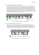
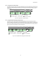
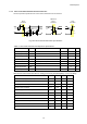
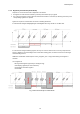
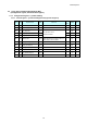
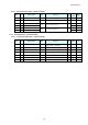
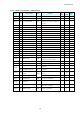
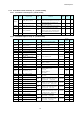
Table Of Contents
- Description
- Features
- Device Structure
- USE RESTRICTION NOTICE
- 1. Block Diagram and Pin Configuration
- 2. Pixel Signal Output Specifications
- 3. Control Registers
- 3-1 2-wire Serial Communication Operation Specifications
- 3-2 2-wire Serial Communication Register Map (Configuration register, Parameter limit register)
- 3-3 Parameter Limit Registers – [0x1000-0x1FFF] (Read Only and Static)
- 3-4 Manufacturer Specific Registers – [0x3000-0x5FFF ]
- 3-5 Frame Bank A and Bank B specific output samples
- 4. Output Data Format
- 6. On Chip Image Processing
- 7. NVM Memory Map
- 8. How to operate IMX219PQH5-C
- 9. Other Functions
- 10. Electrical Characteristics
- 11. Spectral Sensitivity Characteristic
- 12. Image Sensor Characteristics
- 13. Measurement Method for Image Sensor Characteristics
- 14. Spot Pixel Specification
- 15. Notice on White Pixels Specifications
- 16. Chief Ray Angle Characteristics
- 17. Connection Example
- 18. Notes On Handling

IMX219PQH5-C
29
3-2-2-2 Output Set-up Registers – [0x0110-0x0147]
Index
Byte
Register Name
RW
Comment
Re-
Time
Default
(HEX)
Embd
DL
0x0110
[1:0]
CSI_CH_ID
RW
CSI-2 channel ID
0
0x0111
[1:0]
CSI_SIG_MODE
RO
CSI-2 signalling mode
0
0x0114
[1:0]
CSI_LANE_MODE
RW
CSI_lane_mode
0: Reserved, 1: 2-Lane, 2: Reserved,
3: 4-Lane
3
0x0118
[0]
TCLK_POST[8]
RW
Global Timing Parameters
0
0x0119
[7:0]
TCLK_POST[7:0]
RW
Global Timing Parameters
6F
0x011A
[0]
THS_PREPARE[8]
RW
Global Timing Parameters
0
0x011B
[7:0]
THS_PREPARE[7:0]
RW
Global Timing Parameters
2F
0x011C
[0]
THS_ZERO_MIN[8]
RW
Global Timing Parameters
0
0x011D
[7:0]
THS_ZERO_MIN[7:0]
RW
Global Timing Parameters
57
0x011E
[0]
THS_TRAIL[8]
RW
Global Timing Parameters
0
0x011F
[7:0]
THS_TRAIL[7:0]
RW
Global Timing Parameters
2F
0x0120
[0]
TCLK_TRAIL_MIN[8]
RW
Global Timing Parameters
0
0x0121
[7:0]
TCLK_TRAIL_MIN[7:0]
RW
Global Timing Parameters
2F
0x0122
[0]
TCLK_PREPARE[8]
RW
Global Timing Parameters
0
0x0123
[7:0]
TCLK_PREPARE[7:0]
RW
Global Timing Parameters
2F
0x0124
[0]
TCLK_ZERO[8]
RW
Global Timing Parameters
0
0x0125
[7:0]
TCLK_ZERO[7:0]
RW
Global Timing Parameters
BF
0x0126
[0]
TLPX[8]
RW
Global Timing Parameters
0
0x0127
[7:0]
TLPX[7:0]
RW
Global Timing Parameters
27
0x0128
[0]
DPHY_CTRL
RW
MIPI Global timing setting
0: auto mode, 1: manual mode
1
0x012A
[7:0]
EXCK_FREQ[15:8]
RW
INCK frequency [MHz]
0C
0x012B
[7:0]
EXCK_FREQ[7:0]
RW
INCK frequency [MHz]
00
0x0140
[7]
TEMPERATURE_EN
RW
start register to measure sensor
temperature
0
[6:0]
TEMPERATURE_VAL
RO-D
result of measurement of sensor
temperature
XX
0x0142
[7:0]
READOUT_V_CNT
[15:8]
RO-D
indicates current V-counter value for
read-out
XX
0x0143
[7:0]
READOUT_V_CNT[7:0]
XX
0x0144
[0]
VSYNC_POL
RW
defines polarity of V-sync signal.
0: Lo-active, 1: Hi-active
0
0x0145
Reserved
0x0146
[0]
FLASH_POL
RW
defines polarity of flash strobe signal.
0: Hi-active, 1: Lo-active
0
0x0147
[0]
VSYNC_TYPE
RW
Vsync type control
0: Vsync, 1: Reserved
0