
Low Distortion IMX219 M12 Mount Camera Module for Raspberry Pi - Datasheet
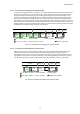
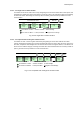
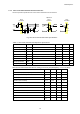
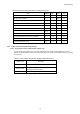
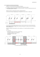
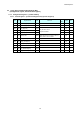
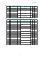
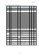
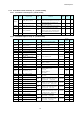
Table Of Contents
- Description
- Features
- Device Structure
- USE RESTRICTION NOTICE
- 1. Block Diagram and Pin Configuration
- 2. Pixel Signal Output Specifications
- 3. Control Registers
- 3-1 2-wire Serial Communication Operation Specifications
- 3-2 2-wire Serial Communication Register Map (Configuration register, Parameter limit register)
- 3-3 Parameter Limit Registers – [0x1000-0x1FFF] (Read Only and Static)
- 3-4 Manufacturer Specific Registers – [0x3000-0x5FFF ]
- 3-5 Frame Bank A and Bank B specific output samples
- 4. Output Data Format
- 6. On Chip Image Processing
- 7. NVM Memory Map
- 8. How to operate IMX219PQH5-C
- 9. Other Functions
- 10. Electrical Characteristics
- 11. Spectral Sensitivity Characteristic
- 12. Image Sensor Characteristics
- 13. Measurement Method for Image Sensor Characteristics
- 14. Spot Pixel Specification
- 15. Notice on White Pixels Specifications
- 16. Chief Ray Angle Characteristics
- 17. Connection Example
- 18. Notes On Handling

IMX219PQH5-C
23
3-1-3 2-wire serial communication block characteristics
The block operation specifications for 2-wire serial communication are show below.
Fig. 18 2-wire Serial Communication Specifications
Table 7 2-wire Serial Communication Operation Specifications
Item
Symbol
Conditions
Min.
Max.
Unit
Low level input voltage
VIL
-0.5
0.3VDIG
V
High level input voltage
VIH
0.7VDIG
VDIG+0.5
V
Low level output voltage
VOL
VDIG < 2 V,Sink 2 mA
0.25VDIG
V
High level output voltage
VOH
VDIG < 2 V,Sink 2 mA
0.75VDIG
V
Output fall time
tof
Load 10 pF 400 pF,0.7VDIG 0.3VDIG
120
ns
Input current
II
0.1VDIG -0.9VDIG
-10
10
µA
SDA I/O capacitance
CI/O
8
pF
SCL Input capacitance
CI
6
pF
Table 8 2-wire Serial Communication AC Timing (Fast mode plus (INCK[fSCK] = 11.4 to 27 MHz))
Item
Symbol
Min.
Max.
Unit
SCL clock frequency ( INCK[fSCK] = 11.4 to 27 MHz)
f
SCL
0
1000
kHz
Rise time (SDA and SCL)
t
R
―
120
ns
Fall time (SDA and SCL)
t
F
―
120
ns
Hold time (start condition)
t
HDSTA
0.26
―
µs
Setup time (rep.-start condition)
t
SUSTA
0.26
―
µs
Setup time (stop condition)
t
SUSTO
0.26
―
µs
Data setup time
t
SUDAT
50
―
ns
Data hold time
t
HDDAT
0
―
µs
Bus free time between Stop and Start condition
t
BUF
0.5
µs
Low period of the SCL clock
t
LOW
0.5
µs
High period of the SCL clock
t
HIGH
0.26
µs
SDA
SCL
t
R
t
F
t
BUF
t
HDSTA
t
LOW
t
SUDAT
t
HIGH
t
HDDAT
t
SUSTA
t
HDSTA
t
SUSTO
Start
Condition
Repeated
Start
Condition
Stop
Condition