
Low Distortion IMX219 M12 Mount Camera Module for Raspberry Pi - Datasheet
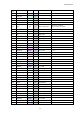
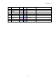

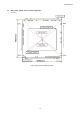
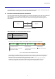
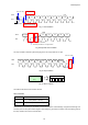
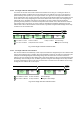
Table Of Contents
- Description
- Features
- Device Structure
- USE RESTRICTION NOTICE
- 1. Block Diagram and Pin Configuration
- 2. Pixel Signal Output Specifications
- 3. Control Registers
- 3-1 2-wire Serial Communication Operation Specifications
- 3-2 2-wire Serial Communication Register Map (Configuration register, Parameter limit register)
- 3-3 Parameter Limit Registers – [0x1000-0x1FFF] (Read Only and Static)
- 3-4 Manufacturer Specific Registers – [0x3000-0x5FFF ]
- 3-5 Frame Bank A and Bank B specific output samples
- 4. Output Data Format
- 6. On Chip Image Processing
- 7. NVM Memory Map
- 8. How to operate IMX219PQH5-C
- 9. Other Functions
- 10. Electrical Characteristics
- 11. Spectral Sensitivity Characteristic
- 12. Image Sensor Characteristics
- 13. Measurement Method for Image Sensor Characteristics
- 14. Spot Pixel Specification
- 15. Notice on White Pixels Specifications
- 16. Chief Ray Angle Characteristics
- 17. Connection Example
- 18. Notes On Handling

IMX219PQH5-C
20
3-1-2-1 CCI single read from random location
The sensor has an index function that indicates which address it is focusing on. In reading the data at an
optional single address, the Master must set the index value to the address to be read. For this purpose it
performs dummy write operation up to the register address. The upper level of the figure below shows the
sensor internal index value, and the lower level of the figure shows the SDA I/O data flow. The Master sets the
sensor index value to M by designating the sensor slave address with a write request, then designating the
address (M). Then, the Master generates the start condition. The Start condition is generated without
generating the Stop condition, so it becomes the Repeated Start condition. Next, when the Master sends the
slave address with a read request, the sensor outputs an Acknowledge immediately followed by the index
address data on SDA . After the Master receives the data, it generates a Negative Acknowledge and the Stop
condition to end the communication.
Fig. 12 CCI single read from random location
3-1-2-2 CCI single read from current location
After the slave address is transmitted by a write request, that address is designated by the next communication
and the index holds that value. In addition, when data read/write is performed, the index is incremented by the
subsequent Acknowledge/Negative Acknowledge timing. When the index value is known to indicate the
address to be read, sending the slave address with a read request allows the data to be read immediately after
Acknowledge. After receiving the data, the Master generates a Negative Acknowledge and the Stop condition
to end the communication, but the index value is incremented, so the data at the next address can be read by
sending the slave address with a read request.
Fig. 13 CCI single read from current location
Register
Address
[15:8]
Register
Address
[7:0]
Data
[7:0]
From Master to Slave
From Slave to Master
S=Start Condition P=Stop Condition
Sr=Repeated Start Condition
A=Acknowledge
A=Negative Acknowledge
Slave
Address
[7:1]
0
AS A A
A
P
Slave
Address
[7:1]
1
A
S
r
Previous Index value Index M
Index
M+1
Index, value M
From Master to Slave
From Slave to Master
S=Start Condition
P=Stop Condition
A=Acknowledge
A=Negative Acknowledge
Slave
Address
[7:1]
1
AS
Previous Index value,K Index K+1
Index
K+2
Data
[7:0]
A
P
Slave
Address
[7:1]
1
AS
Data
[7:0]
A
P