
Low Distortion IMX219 M12 Mount Camera Module for Raspberry Pi - Datasheet
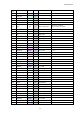


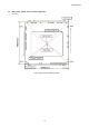
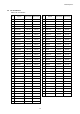
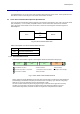
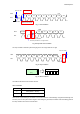
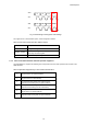
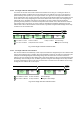
Table Of Contents
- Description
- Features
- Device Structure
- USE RESTRICTION NOTICE
- 1. Block Diagram and Pin Configuration
- 2. Pixel Signal Output Specifications
- 3. Control Registers
- 3-1 2-wire Serial Communication Operation Specifications
- 3-2 2-wire Serial Communication Register Map (Configuration register, Parameter limit register)
- 3-3 Parameter Limit Registers – [0x1000-0x1FFF] (Read Only and Static)
- 3-4 Manufacturer Specific Registers – [0x3000-0x5FFF ]
- 3-5 Frame Bank A and Bank B specific output samples
- 4. Output Data Format
- 6. On Chip Image Processing
- 7. NVM Memory Map
- 8. How to operate IMX219PQH5-C
- 9. Other Functions
- 10. Electrical Characteristics
- 11. Spectral Sensitivity Characteristic
- 12. Image Sensor Characteristics
- 13. Measurement Method for Image Sensor Characteristics
- 14. Spot Pixel Specification
- 15. Notice on White Pixels Specifications
- 16. Chief Ray Angle Characteristics
- 17. Connection Example
- 18. Notes On Handling

IMX219PQH5-C
19
Fig. 11 Acknowledge and Negative Acknowledge
The registers have a 16-bit address space, and are assigned as follows.
Table 5 2-wire Serial Communication Address Space
Address area
Description
0x0000 - 0x0FFF
Configuration register
0x1000 - 0x1FFF
Parameter limit register
Read Only and Static register
0x3000 - 0xFFFF
Manufacture specific register
3-1-2 2-wire serial communication read/write operation supported
The IMX219PQH5-C supports the following four read operations and two write operations that conform to the
SMIA standard.
Table 6 Operations Supported by 2-wire Serial Communication
1
CCI Single read from random location
(Single read from an optional address)
2
CCI Single read from current location
(Single read from the held address)
3
CCI sequential read starting from random location
(Sequential read starting from an optional address)
4
CCI sequential read starting from current location
(Sequential read starting from the held address)
5
CCI single write to random location
(Single write to an optional address)
6
CCI sequential write starting from random location
(Sequential write starting from an optional address)
D1 D0 R/W
SDA SCL
ACK
D1 D0 R/W
SDA SCL
NACK
SDA
SCL
SDA
SCL