
Data Sheet

10.13.2009 PRODUCT SPECIFICATION proprietary to OmniVision Technologies
7-1
7 register tables
The following tables provide descriptions of the device control registers contained in the OV7675/OV7175. For all register
enable/disable bits, enable = 1 and DISABLE = 0. The device slave addresses are 0x42 for write and 0x43 for read.
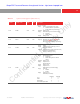
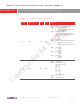
table 7-1 system control registers (sheet 1 of 17)
address
register name
default
value
R/W
description
0x00 GAIN 0x00 RW
AGC - Gain Control Gain Setting
Bit[7:0]: AGC[7:0] (see VREF[7:6] (0x03) for
AGC[9:8])
0x01 BLUE 0x80 RW
AWB – Blue Channel Gain Setting
Blue Gain = BLUE[7:0] / 0x40, BLUE[7:0] ≥ 0x40
0x02 RED 0x80 RW
AWB – Red Channel Gain Setting
Red Gain = RED[7:0] / 0x40, RED[7:0] ≥ 0x40
0x03 VREF 0x00 RW
Vertical Frame Control
Bit[7:6]: AGC[9:8] (see GAIN[7:0] (0x00) for
AGC[7:0])
Bit[5:4]: Debug mode
Bit[3:2]: VREF end 2 LSBs (8 MSBs at
VSTART[7:0] (0x19))
Bit[1:0]: VREF start 2 LSBs (8 MSBs at
VSTOP[7:0] (0x1A))
0x04 COM1 0x00 RW
Common Control 1
Bit[7]: Debug mode
Bit[6]: CCIR656 format
0: Disable
1: Enable
Bit[5:2]: Debug mode
Bit[1:0]: 2 LSBs (see registers AECHH[5:0]
(0x07) and AECH[7:0] (0x10) for
AEC[15:10] and AEC[9:2], respectively)
0x05 BAVE 0x00 RW
U/B Average Level
Automatically updated based on chip output format
0x06 BGAVE 0x00 RW
Y/Gb Average Level
Automatically updated based on chip output format
0x07 AECHH 0x00 RW
Exposure Value - AEC 5 MSBs
Bit[7:6]: Not used
Bit[5:0]: AEC[15:10] (see registers AECH[7:0]
(0x10) and COM1[1:0] (0x04) for
AEC[9:2] and AEC[1:0], respectively)
gain = (0x03[7] + 1) x (0x03[6] + 1) x (0x00[7] + 1) (0x00[6] + 1) x
(0x00[5] + 1) x (0x00[4] + 1) x ( + 1)
0x00[3:0]
16
Simpo PDF Password Remover Unregistered Version - http://www.simpopdf.com