
Data Sheet

10.13.2009 PRODUCT SPECIFICATION proprietary to OmniVision Technologies
2-3
2.1 format and frame rate
The OV7675/OV7175 supports the following formats YUV422, RAW RGB, ITU656, and RGB565.
2.2 power up sequence
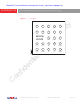
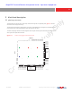
2.2.1 power up with internal DVDD
When powering up with the internal DVDD and SCCB access during the power ON period, the following conditions must
occur:
1. if V
DD-IO
and V
DD-A
are turned ON at the same time, make sure V
DD-IO
becomes stable before V
DD-A
becomes stable
2. PWDN is active high with an asynchronized design (does not need clock)
3. PWDN must go high during the power up period
4. for PWDN to go low, power up must first become stable (AVDD to PWDN >
5 ms)
5. master clock XVCLK should provide at least 1 ms before host accesses sensor’s I2C
6. host can access I2C bus (if shared) during entire period. 20 ms after PWDN goes low goes high if reset is
inserted after PWDN goes low, host can access sensor’s SCCB to initialize sensor
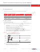
figure 2-3 power up timing with internal DVDD
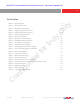
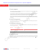
table 2-1 format and frame rate
format resolution frame rate scaling method pixel clock (YUV/RAW)
VGA 640x480 30 fps full 24/12 MHz
QVGA 320x240 60 fps sub sampling from VGA 24/12 MHz
QQVGA 160x120 240 fps
cropped and window from
center of VGA
24/12 MHz
VDD_IO
(DOVDD)
VDD_A
(AVDD)
SCCB activity is okay during entire period
power down
VDD
_
IO first, then VDD_A, and rising time is less than 5 ms
PWDN
SCCB
note T0 ≥ 0 ms: delay from VDD_IO stable to VDD_A stable
T2 ≥ 5 ms: delay from VDD_A stable to sensor power up stable
if PWDN is not used, sensor SCCB is accessible after TO + T2
T0
T2
power on period
7675_DS_2_3
Simpo PDF Password Remover Unregistered Version - http://www.simpopdf.com