
User's Manual

APPLIED TECHNOLOGY SOLUTIONS, INC.
DOCUMENT: fcc1250MAN.wpd ISSUED:jan99 REVISED: (ORIGINAL) PAGE: 8
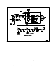
the spread data signal, which along with the PN sequence, is biphase modulated by the clock signal from the modulator clock
generator. Further processing of these signals occurs outside the FPGA.
Two clock generator circuits are included in the FPGA, both being driven from the same crystal oscillator stage.
The data clock generator has three outputs, the PN clock, the scrambler clock and the CVSD clock. The modulator clock
generator has two outputs, one being twice the frequency of the other, driving the biphase modulators.
4.1.2 IF/RF Section
The two biphase modulated signals from the FPGA are individually bandpass filtered, and then added together, to
produce the baseband composite spread spectrum signal. This signal is up-converted at the first IF (Intermediate Frequency)
mixer. The output from the first IF mixer is bandpass filtered to remove mixer image products.
The first IF signal is up-converted to the final transmit frequency by the second IF mixer. The output of the second
IF mixer is also bandpass filtered and drives the RF power amplifier. Prior to going to the antenna, the output signal from
the RF power amplifier is lowpass filtered, to remove any harmonics generated by the RF power amplifier.
4.2 RF CHARACTERISTICS
The Series 1250 Transmitter is a low power, transmit only device, therefore its operating range is more sensitive
to the physical and electrical environment. The transmit range from a 1250 to a receiver should approximate 200 feet for
a fixed installation and 100 feet if placed on a body. The actual range is dependent on many factors and ATS recommends
the installation be verified before deployment. Placing the Model 1240 Portable Repeater to the Repeater/Transceiver
functional mode and using a PTT transmitter is the easiest way to verify receive and transmit capability. When this is not
possible, the repeater should be placed within 100 feet of a Series 1250 Transmitter.