
User`s guide


Frequently Asked Questions
B-3
market. Also, there is no chipset that can support P1394. Probably in the
near future, a card will be developed to support P1394 device.
Q: What is SMBus (System Management Bus, also called I2C bus)?
A: SMBus is a two-wire bus developed for component communication
(especially for semiconductor IC). It is most useful for notebook to detect
component status and replace hardware configuration pin (pull-high or pull-
low). For example, disabling clock of DIMM that does not exist, or detecting
battery low condition. The data transfer rate of SMBus is only 100Kbit/s, it
allows one host to communicate with CPU and many masters and slaves to
send/receive message. The SMBus may be used for jumpless mainboard,
the components which support SMbus are not ready yet, we will keep eyes
on it.
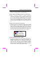
Q: What is FCC DoC (Declaration of Conformity)?
A: The DoC is new certif ication standard of FCC regulations. This new standard
allows DIY component (such as mainboard) to apply DoC label separately
without a shielding of housing. The rule to test mainboard for DoC is to
remove housing and test it with regulation 47 CFR 15.31. The DoC test of
mainboard is more difficult than traditional FCC test. If the mainboard
passes DoC test, that means it has very low EMI radiation and you can use
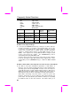
any kind of housing (even paper housing). Following is an example of DoC
label. Currently, AOpen AX65/AP57/AP5T/AX5T had passed DoC test.
AX5T
Test To Comply
With FCC Standards
FOR HOME OR OFFICE USE
Q: What is PBSRAM (Pipelined Burst SRAM)?
A: For Pentium CPU, the Burst means reading four QWord (Quad-word, 4x16 =
64 bits) continuously with only the first address decoded by SRAM. The
PBSRAM will automatically send the remaining three QWord to CPU
according to predefined sequence. The normal address decoding time for
SRAM is 2 to 3 clocks. This makes the CPU data read timing of four QWord
to be at least 3-2-2-2 and a total of 9 clocks if traditional asynchronous
SRAM is used. However, with PBSRAM, there is no need to decode address
for rest three Qword. Therefore, data read timing can be 3-1-1-1, that is
equivalent to 6 clocks and is faster than asynchronous SRAM.