21.5" LCD Color Monitor AOC E2251SWDN Service Service Service Horizontal Frequency 30-83KHz Table of Contents Description Page Description Page Table of Contents.......……..............................……........1 5.Block Diagram…….........………….................25 Revision List.…........................................…………........2 6.Schematic……………........................................26 Important Safety Notice.……............................……......3 6.1.Main Board………............................
Revision List Version Release Date Revision History L&T Model Name TIBJT32CB7SUHNF.LF A00 Jun-5-2012 Initial Release TIBJT32KB7A1HNF.LF TIBJT32CB7JBHNF.LF A01 AUG-20-2012 Add new models 2 TIBJT32EB7RMHNF.LF TIBJT32EB7SPHNF.
Important Safety Notice Proper service and repair is important to the safe, reliable operation of all AOC Company Equipment. The service procedures recommended by AOC and described in this service manual are effective methods of performing service operations. Some of these service operations require the use of tools specially designed for the purpose. The special tools should be used when and as recommended.
1.
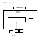
2. LCD Monitor Description The LCD MONITOR will contain a main board and a key board which house the flat panel control logic, brightness control logic and DDC. Monitor Block Diagram Flat Panel and LED Drive.
3. Operating Instructions 3.1 General Instructions Press the power button to turn the monitor on or off. The other control knobs are located at front panel of the monitor. By changing these settings, the picture can be adjusted to your personal preferences. 3.2 Hotkeys Power Press the Power button to turn on/off the monitor. Menu/Enter Press to display the OSD or confirm the selection Eco (DCR)/Press the Eco key continuously to select the Eco mode of brightness and DCR on when there is no OSD.
3.3 OSD Setting Basic and simple instruction on the control keys. 1) Press the MENU-button to activate the OSD window. 2) Press < or > to navigate through the functions. Once the desired function is highlighted, press the MENU-button to activate sub-menu . Once the desired function is highlighted, press MENU-button to activate it. 3) Press or to change the settings of the selected function. Press AUTO to exit. If you want to adjust any other function, repeat steps 2-3.
Luminance 1 Press (Menu) to display menu 2 Press or to select (Luminance), and press to enter 3 Press or to select submenu, and press to enter.
4 Press or to adjust 5 Press to exit.
Image Setup 1 Press (Menu) to display menu 2 Press or to select (Image Setup) , and press or to select submenu, and press or to adjust. 3 Press to enter. 4 Press 10 to enter.
5 to exit. Press Clock 0-100 Adjust picture Clock to reduce Vertical-Line noise. Phase 0-100 Adjust Picture Phase to reduce Horizontal-Line noise Sharpness 0-100 Adjust picture sharpness H.Position 0-100 Adjust the horizontal position of the picture. V.Position 0-100 Adjust the vertical position of the picture. Color Setup 1 Press (Menu) to display menu. 2 Press or to select (Color Setup), and press 11 to enter.
3 Press or to select submenu, and press or to adjust. to enter. 4 Press 5 Press to exit.
Color setup. Warm Recall Warm Color Temperature from EEPROM. Normal Recall Normal Color Temperature from EEPROM. Cool Recall Cool Color Temperature from EEPROM. sRGB Recall SRGB Color Temperature from EEPROM. Red Red Gain from Digital-register Green Green Gain Digital-register.
Press or to select submenu, and press or to adjust. to enter. 4 Press 5 Press to exit. Frame Size 14-100 Adjust Frame Size Brightness 0-100 Adjust Frame Brightness Contras 0-100 Adjust Frame Contrast H. position 0-100 Adjust Frame horizontal Position V.
OSD Setup 1 Press (Menu) to display menu. 2 Press or to select (OSD Setup), and press or to select submenu, and press to enter. 3 Press 15 to enter.
4 Press or to adjust. 5 Press to exit. H.Position 0-100 Adjust the horizontal position of OSD V.Position 0-100 Adjust the vertical position of OSD Timeout 5-120 Adjust the OSD Timeout Transparence 0-100 Adjust the transparence of OSD Language Select the OSD language Extra 1 Press (Menu) to display menu.
2 Press or to select (Extra), and press or to select submenu, and press or to adjust. to enter. 3 Press to enter. 4 Press 5 Press to exit.
Exit 1 Press (Menu) to display menu. 2 Press or to select (Exit), and press to exit.
4. Input/Output Specification 4.1 D-SUB CONNECTORS Pin Assignments Pin Number 15-Pin Side of the Signal Cable Pin Number 9 15-Pin Side of the Signal Cable +5V 1 Video-Red 2 Video-Green 10 Ground 3 Video-Blue 11 N.C. 4 N.C.
4.
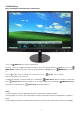
4.3 Panel Specification 4.3.1 General Features BM215WF4-T2BB is a Color Active Matrix Liquid Crystal Display with an integral Light Emitting Diode (LED) backlight system. The matrix employs a-Si Thin Film Transistor as the active element. It is a transmissive type display operating in the normally white mode. It has a 21.
4.3.3 Electrical Characteristics Ta = 25°C Values Parameter Symbol Unit Min Typ Max Notes MODULE : Power Supply Input Voltage VLCD 4.5 5.0 5.5 Vdc Permissive Power Input Ripple VLCD - - 0.3 V 3 ILCD-MOSAIC(60Hz) - 1000 1300 mA 1,5 ILCD-BLACK(60Hz) - 1300 1690 mA 2,5 - 2000 mA 5 Power Supply Input Current ILCD-BLACK(75Hz) Power Consumption PLCD - 5.00 6.5 Watt 1 Inrush current IRUSH - - 3.
4.3.4 Optical Characteristics (Ta=25 °C, VLCD=5.0V, fV=60Hz, DCLK=72MHz, Is=110mA) Values Parameter Symbol Units Min Typ Max 1 Contrast Ratio CR 400 600 - Surface Luminance, white LWH 160 200 - cd/m2 75 - - % Luminance Variation WHITE 9P Notes (PR-880) 2 (PR-880) 3 (PR-880) Rise Time TrR - 1.3 2.6 ms 4 Decay Time TrD - 3.7 7.4 ms (RD80S) Response Time Rx 0.642 Ry 0.332 Gx 0.305 RED GREEN Color Coordinates Gy Typ 0.625 Typ [CIE1931] Bx -0.03 0.150 +0.
5. Block Diagram 5.1 Main Board CRYSTAL Panel Interface 14.
6. Schematic 6.1 Main Board 715G4798M0E000004L D-SUB 15P VGA_CABLE_DET 16 CN101 DDCSCL1 R101 DDCSCL_A 47R 1/16W 5% VSIN0 DDCSDA1 DDCSDA1 R105 DDCSDA_A 47R 1/16W 5% 12 11 BIN0BIN0 GIN0GIN0 RIN0RIN0 FB104 1 BIN0 ZD101 R104 10R 1/16W 5% 2 C102 B0+ BEAD B0+ 5 B0- 5 47nF 16V RLZ5.
PA[0..9] PA[0..9] 5 PA0 PA1 PA2 PA3 PA4 PA5 PA6 PA7 PA8 PA9 PB[0..9] PB[0..
U703 3 2 VOUT 1 GND VIN 3 2 1 VIN VOUT(TAB) ADJ(GND) U702 G1117-33T43UF +5V SOT 223 FB702 1 VCC3.3 U701 3 2 VI VO Dropout voltage must < 0.
2 120 OHM C409 100N16V C424 10uF 10V EESCL EESDA NC/22K 1/16W 5% NC/4K7 1/16W 5% V12C R406 NC/100R 1/16W 5% U402 8 7 6 5 R404 V33TMDS LVA0M LVA0P LVA1M LVA1P LVA2M LVA2P LVACKM LVACKP LVA3M LVA3P R403 FB404 1 2 120 OHM PA9 PA8 PA7 PA6 PA5 PA4 PA3 PA2 PA1 PA0 R402 V33P FB403 1 VCC3.3 C408 100N16V VCC3.3 7 LVB3P LVB3M LVBCKP LVBCKM LVB2P LVB2M LVB1P LVB1M LVB0P LVB0M NC/4K7 1/16W 5% VCC3.
+12V 7 L801 R813 1K 1/10W 5% 100N 50V R807 R808 BKLT_VBR1 1K 1/10W 5% R810 20K 1/10W 5% R802 270K +-1% 1/10W C808 NC R803 D1 D1 D2 D2 8 7 6 5 R801 10R 1/8W 5% C805 1000pF 50V OVP Q806 P8008HV + C803 C807 C813 0.47UF 50V 2N2 50V 4.7UF 100V C804 C809 C814 0.47UF 50V 2N2 50V 1000pF 50V R841 2.2OHM 1/10W R805 300K 1/8W 5% R842 2.2OHM 1/10W OVP R843 680 OHM 1/4W C815 R834 C806 R812 0.12R 1% R809 270K +-1% 1/10W 100pF 50V 2010/2/9 R816 NC 6.
6.2 Key Board CIN_03 CIN_01 GPIO_01 GPIO_00 715G4842K0E000004F INT# SDA SCLK DVCC 12 11 10 9 4K7 1/16W 5% R003 SM_INT# SM_DATA SM_CLK C003 12P 50V C004 12P 50V CN001 5 6 7 8 KEY 0.1524 C011 C006 100nF 25V ZD001 UDZSNP5.6B 1UF 10V R005 R006 0R05 1/16W 0R05 1/16W CLK DATA SM_INT# 1 2 3 4 5 6 ZD002 UDZSNP5.6B CABLE 1 1 V3.3 C007 100nF 25V SM_CLK SM_DATA 5V_LED 2 VBIAS V3.3 V3.
7. PCB Layout 7.
7.
8. Maintainability 8.1 Equipments and Tools Requirement 1. Voltmeter. 2. Oscilloscope. 3. Pattern Generator. 4. DDC Tool with an IBM Compatible Computer. 5. Alignment Tool. 6. LCD Color Analyzer. 7. Service Manual. 8. User Manual.
8.2 Trouble Shooting 1.
2.
3.
4.
9. White- Balance, Luminance Adjustment Approximately 30 minutes should be allowed for warm up before proceeding white balance adjustment. How to setting MEM channel you can reference to chroma 7120 user guide or simpl use “SC” key and “NEXT” Key to modify xyY value and use “ID” key to modify the TEXT description Following is the procedure to do white-balance adjust . 2. Setting the color temp. you want A. MEM.CHANNEL 3 Warm (6500K): Warm color temp. parameter is x = 313 ±30, y = 329 ±30 B. MEM.
C. Adjust Cool (9300K) color-temperature 1. Switch the Chroma-7120 to RGB-Mode (with press “MODE” button) 2. Switch the MEM. Channel to Channel 9 (with up or down arrow on chroma 7120) 3. The LCD-indicator on chroma 7120 will show x = 283 ±30, y = 297 ±30 4. Adjust the RED on factory window until chroma 7120 indicator reached the value R=100 5. Adjust the GREEN on factory window until chroma 7120 indicator reached the value G=100 6.
10.
No. Description 1 BEZEL 2 Power lens 3 RUBBER FEET 4 Main frame 5 Rear cover 6 Hinge 7 Stand 8 Stand cover 9 Base No.
11. BOM List Note: The parts information listed below are for reference only, and are subject to change without notice. Please go to http://cs.tpv.com.cn/hello1.asp for the latest information. TIBJT32CB7SUHNF.
3110T-0856A 3110T-0856B 3850L-0088A 4296L-0284B GALVALUME, T=0.3,BM215WF4-TJA1-6F1-A0, Up GALVALUME, T=0.3,BM215WF4-TJA1-6F1-A0, Down ID, YUPO, 78X37 PMP-P2 100-520U-13, 5U-C60 black A600, 170x7x0.45 6060L-2569A LM215WF4(TJBA,T2BB) 6061L-2064A LM215WF4-TJAA 0ILUL-0185A 6308L-4013A 6308L-4014A 6871L-2552B LS0609D3-C6LS, LUSEM, 960, 6BIT, MINI, C_B, R/TP, 48MM, 4PF, UPILEX, T9 LTBXNSSNXX1-02150T01, 487.1*277.5, LGC,T,B,X,N,S, S,N,X,X,1,02150,Top,01 LTXXNSSNXX1-02150B01, 487.10*277.
C77,C907 C73 0CH2A-0017A 2.2U F, 10 Volt, K PER, X5R(JB), 1608 R/TP, T=0.9(MAX) C313,C314,C3 15,C318,C52, C61,C62,C63, C64,C71,C72, 0CH2A-0026A 10U F, 25 Volt, K PER, X5R(JB), 3225 R/TP, T=1.0(MAX) C913,C914,C9 20,C921 0.1U F, 25 Volt, Z PER, Y5V(JF), 1005 R/TP, C312 0CH2A-0038A C701 0CH2A-0049A 1.5nF, 50, -10~+10(K), 1608, X7R(JB) C75 0CH2A-0088A 3.3nF, K, 50V, X7R, 0.9mm, 1608, R/TP C912 0CH2A-0091A 1uF, K, 25V, X5R, 0.
R140,R142,R1 79,R180,R20, R302,R54,R60 1,R602,R801, R802,R901,R9 02,R903,R906, R908 R131 0RH0102C422 10 OHM 1/16W 1608 1% D R/TP R701 0RH0221C622 2.2 OHM 1/16W 1608 5% D R/TP 0RH0302C422 30 OHM 1/16W 1608 1% D R/TP R322 0RH0472C422 47 OHM 1/16W 1608 1% D R/TP R2,R3 0RH1000C422 100 OHM 1/16W 1608 1% D R/TP R1 0RH1001C422 1K OHM 1/16W 1608 1% D R/TP R24,R55 0RH1002C422 10K OHM 1/16W 1608 1% D R/TP 0RH1102C422 11K OHM 1/16W 1608 1% D R/TP R214 0RH1201C422 1.
R243,R253 0RH2702C422 27K OHM 1/16W 1608 1% D R/TP 0RH3302C422 33K OHM 1/16W 1608 1% D R/TP R135 0RH3602C422 36K 1/16W 1% 1608 R201 0RH3900C422 390 OHM 1/16W 1608 1% D R/TP R146 0RH3902C422 39K OHM 1/16W 1608 1% D R/TP 0RH4700C422 470 OHM 1/16W 1608 1% D R/TP 0RH4702C422 47K OHM 1/16W 1608 1% D R/TP 0RH5101C422 5.1K OHM 1/16W 1608 1% D R/TP R117 0RH5102C422 51K OHM 1/16W 1608 1% D R/TP R203 0RH5600C422 560 ohm, 1/16W, 1608, 1%, R/TP 0RH5601C422 5.
CN1 6630L-0157B 6630L-0410A 6870S-1235A E2436L FI-XB30SL-HF10, JAE, 30 Pin, 1 mm, Angle, Sn, USER LOCK IS100-L30F-C15, UJU, 30 Pin, 1 mm, Angle, Sn, USER LOCK LM215WF4-TJC1-611, 2L, 0.6, 479.15*122.15, 3, N, Source, NO, Single Side 6091L-1904D BM215WF4-T2AA 6091L-1904B BM215WF4-T2AA 3022L-1413A KOLON, XC210, T=0.123, BM215WF4-TJA1-6F1-A0 3022L-1413B LUCKY, CDX131, T=0.21, BM215WF4-TJA1 3550B-0918A AL, T=0.
7250L-1408A 7250L-1488B SMTCA-U403 15*25*0.11 MAINBOARD-CBPCAT3A1AX 100GARJI004FT1 MCU ASS’Y-056G2233-11 A15G1636101 MAIN_FRAME A15G1648101 PlATE A33G1203AED-1B0100 stand-top A33G1204--1-1C0100 Power lens 0 C716 Conductive Tape,STN1026WR(P), T=0.11, 756GFBCB-AA016--00 A34G2579AEDD1B013 CN406 ZH350 25x16x0.1 BEZEL A34G2580AED-1B0100 rear cover A34G2581AED-1B0100 Stand-cover A34G2618AED-1B0130 BASE A37G0252011 HINGE 033G801930F-CH---L WAFER 30P 1.
055G--23524--A WELDING FULX WITHOUT Pb Q49G--51100 GW2066 Cleaner Q55G-100625 TIN STICK_LOW ARGENTUM F67G305M1013GV 100uF +-20% 16V 105 ℃ 2000H 6.3*7 067G305S1013HV EC 100UF 20% 16V 6.3*7 F88G-304-11-YG DC JACK 3P BLACK YCG 088G-304-11--C DC JACK 3P BLACK CL 033G801910Y--H NO-SUGGEST WAFER 10P 0.5MM GAOLIN 311GF050B10ADH FFC CONN 10P 0.5MM HR U401 056G-562434 IC SCALER RTD2281W-CG QFP-128 Realtek U702 056G-563512--C IC LDO G1117-33PT43U 1A 3.
Q705 057G-763535 MOSFET LP3401LT1G -4.2A/-30V SOT-23 LRC 057G-763940 MOSFET AO3401A 4.
77,R478 R112,R113,R1 28,R129,R415, R420,R451,R4 59,R467,R475, 061G0402472-JT RST CHIPR 4.
R843 061G1206681-JT RST CHIPR 680 OHM +-5% 1/4W 065G040210131J---Y MLCC 0402 100pF +-5% 50V NPO YAGEO 065G040210412K---A MLCC 0402 0.1uF +-10% 16V X7R SAMSUNG 065G0402105A5K---A MLCC 0402 1uF +-10% 10V X5R SAMSUNG 065G0402105A5K---T MLCC 0402 1uF -10% 10V X5R TAIYO YUDEN 065G040222031J---T MLCC 0402 22pF +-5% 50V NPO TAIYO YUDEN C722 065G040222232K---Y MLCC 0402 2.
065G060347412K---T C802 C413,C424,C4 25 MLCC 0603 68nF +-10% 50V X7R YAGEO 065G0805106A5K---A MLCC 0805 10uF +-10% 10V X5R SAMSUNG C813,C814 065G080522232K---Y C803,C804 065G080547432K---T FB102,FB403, FB404,FB702 FB408 FB104,FB105, FB106 L801 D101,D102 YUDEN MLCC 1206 10uF -10% 25V X5R TAIYO YUDEN 070GHDCP500HDC HDCP CODE 071G-56K121--M CHIP BEAD 071G-59G301-TA 071G-59K190-TA 2nd SOURCE 2nd SOURCE CHIP BEAD 0603 120R 25% 300mA FCM1608CF-121T03 TAI-TECH FCM1608C-121T03 SMD 2nd SOURCE
DIDOE ZD ZM-PTZ9.1BST 9.1V/1W LL-41 ZD703 093G-39GA52--T D801 093G-60S907--T D701 093G3004--2 DIODE SCHOTTKY SR34 3A/40V SMB PANJIT 311GF100C06ADH FFC CONN 6P 1.0mm CN405 U705 356G0563419 056G-563513 E715 Diode SCHOTTKY B3100B 3A 100V SMB LITEON HR IC LDO DC/DC APW7089KAI-TRG 4A 26V SOP-8P ANPEC NO-SUGGEST IC LDO APW7080KAITRG 4A/26V SOP-8P ANPEC 2nd SOURCE 709G4798-QS001 COMSUPTIVE ASS""Y 052G---2191--A PAPER TAPE 715G4798M01000004L MAIN PCB FR-4 92*102mm*1.
F95G176X-10103 FFC CABLE 10P 326MM P0.5MM WENXIN F95G179X30N102 FFC CABLE 30P 241MM P1.0MM WENXIN F95G179J30N102 FFC CABLE 30P 241MM P1.0MM KOTL KEPCAAB5 KEY BOARD F95G-76T--6603 FFC CABLE 6PIN 344MM 1.0MM DIY F95G-76X--6603 FFC CABLE 6PIN 344MM 1.0MM WENXIN 2nd SOURCE F95G-76J--6603 FFC CABLE 6PIN 344MM 1.
E715 715G4842K01000004S Key Board FR-4 105*11*1.2mm 16 715G4842K01000004F Key Board FR-4 105*11*1.2mm 16 2nd SOURCE 715G4842K01000004L Key PCB FR-4 105*11*1.